Flip-flop (electronics)
From Wikipedia, the free encyclopedia

In digital circuits, a flip-flop is a term referring to an electronic circuit (a bistable multivibrator) that has two stable states and thereby is capable of serving as one bit of memory. Today, the term flip-flop has come to mostly denote non-transparent (clocked or edge-triggered) devices, while the simpler transparent ones are often referred to as latches; however, as this distinction is quite new, the two words are sometimes used interchangeably (see history).
A flip-flop is usually controlled by one or two control signals and/or a gate or clock signal. The output often includes the complement as well as the normal output. As flip-flops are implemented electronically, they require power and ground connections.
Contents |
[edit] History
The first electronic flip-flop was invented in 1918 by William Eccles and F. W. Jordan.[1][2] It was initially called the Eccles–Jordan trigger circuit and consisted of two active elements (radio-tubes). The name flip-flop was later derived from the sound produced on a speaker connected to one of the back coupled amplifiers outputs during the trigger process within the circuit (as such, it may be considered a case of onomatopoeia).[citation needed] This original electronic flip-flop—a simple two-input bistable circuit without any dedicated clock (or even gate) signal, was transparent, and thus a device that would be labeled as a "latch" in many circles today.
[edit] Implementation
Flip-flops can be either simple (transparent) or clocked. Simple flip-flops can be built around a pair of cross-coupled inverting elements: vacuum tubes, bipolar transistors, field effect transistors, inverters, and inverting logic gates have all been used in practical circuits — perhaps augmented by some gating mechanism (an enable/disable input). The more advanced clocked (or non-transparent) devices are specially designed for synchronous (time-discrete) systems; such devices therefore ignore its inputs except at the transition of a dedicated clock signal (known as clocking, pulsing, or strobing). This causes the flip-flop to either change or retain its output signal based upon the values of the input signals at the transition. Some flip-flops change output on the rising edge of the clock, others on the falling edge.
Clocked flip-flops are typically implemented as master-slave devices[3] where two basic flip-flops (plus some additional logic) collaborate to make it insensitive to spikes and noise between the short clock transitions; they nevertheless also often include asynchronous clear or set inputs which may be used to change the current output independent of the clock.
Flip-flops can be further divided into types that have found common applicability in both asynchronous and clocked sequential systems: the SR ("set-reset"), D ("data" or "delay"[4]), T ("toggle"), and JK types are the common ones; all of which may be synthesized from (most) other types by a few logic gates. The behavior of a particular type can be described by what is termed the characteristic equation, which derives the "next" (i.e., after the next clock pulse) output, Qnext, in terms of the input signal(s) and/or the current output, Q.
[edit] Set-Reset flip-flops (SR flip-flops)

The fundamental latch is the simple SR flip-flop , where S and R stand for set and reset respectively. It can be constructed from a pair of cross-coupled NOR logic gates. The stored bit is present on the output marked Q.
Normally, in storage mode, the S and R inputs are both low, and feedback maintains the Q and Q outputs in a constant state, with Q the complement of Q. If S (Set) is pulsed high while R is held low, then the Q output is forced high, and stays high even after S returns low; similarly, if R (Reset) is pulsed high while S is held low, then the Q output is forced low, and stays low even after R returns low.
| SR Flip-Flop operation [5] | |||||||
|---|---|---|---|---|---|---|---|
| Characteristic table | Excitation table | ||||||
| S | R | Action | Q(t) | Q(t+1) | S | R | Action |
| 0 | 0 | Keep state | 0 | 0 | 0 | X | No change |
| 0 | 1 | Q = 0 | 0 | 1 | 1 | 0 | Set |
| 1 | 0 | Q = 1 | 1 | 0 | 0 | 1 | Reset |
| 1 | 1 | Unstable combination, see race condition |
1 | 1 | X | 0 | No change |
('X' denotes a Don't care condition; meaning the signal is irrelevant)
[edit] Toggle flip-flops (T flip-flops)

If the T input is high, the T flip-flop changes state ("toggles") whenever the clock input is strobed. If the T input is low, the flip-flop holds the previous value. This behavior is described by the characteristic equation:
 (or, without benefit of the XOR operator, the equivalent:
  )
)
and can be described in a truth table:
| T Flip-Flop operation [5] | ||||||||
|---|---|---|---|---|---|---|---|---|
| Characteristic table | Excitation table | |||||||
| T | Q | Qnext | Comment | Q | Qnext | T | Comment | |
| 0 | 0 | 0 | hold state(no clk) | 0 | 0 | 0 | No change | |
| 0 | 1 | 1 | hold state(no clk) | 1 | 1 | 0 | No change | |
| 1 | 0 | 1 | toggle | 0 | 1 | 1 | Complement | |
| 1 | 1 | 0 | toggle | 1 | 0 | 1 | Complement | |
When T is held high, the toggle flip-flop divides the clock frequency by two; that is, if clock frequency is 4 MHz, the output frequency obtained from the flip-flop will be 2 MHz. This 'divide by' feature has application in various types of digital counters. A T flip-flop can also be built using a JK flip-flop (J & K pins are connected together and act as T) or D flip-flop (T input and Qprevious is connected to the D input through an XOR gate).
[edit] JK flip-flop

The JK flip-flop augments the behavior of the SR flip-flop (J=Set, K=Reset) by interpreting the S = R = 1 condition as a "flip" or toggle command. Specifically, the combination J = 1, K = 0 is a command to set the flip-flop; the combination J = 0, K = 1 is a command to reset the flip-flop; and the combination J = K = 1 is a command to toggle the flip-flop, i.e., change its output to the logical complement of its current value. Setting J = K = 0 does NOT result in a D flip-flop, but rather, will hold the current state. To synthesize a D flip-flop, simply set K equal to the complement of J. The JK flip-flop is therefore a universal flip-flop, because it can be configured to work as an SR flip-flop, a D flip-flop, or a T flip-flop. NOTE: The flip flop is positive edge triggered (Clock Pulse) as seen in the timing diagram.

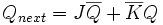
The characteristic equation of the JK flip-flop is:
and the corresponding truth table is:
| JK Flip Flop operation [5] | ||||||||
|---|---|---|---|---|---|---|---|---|
| Characteristic table | Excitation table | |||||||
| J | K | Qnext | Comment | Q | Qnext | J | K | Comment |
| 0 | 0 |  |
hold state | 0 | 0 | 0 | X | No change |
| 0 | 1 |  |
reset | 0 | 1 | 1 | X | Set |
| 1 | 0 |  |
set | 1 | 0 | X | 1 | Reset |
| 1 | 1 |  |
toggle | 1 | 1 | X | 0 | No change |
The origin of the name for the JK flip-flop is detailed by P. L. Lindley, a JPL engineer, in a letter to EDN, an electronics design magazine. The letter is dated June 13, 1968, and was published in the August edition of the newsletter. In the letter, Mr. Lindley explains that he heard the story of the JK flip-flop from Dr. Eldred Nelson, who is responsible for coining the term while working at Hughes Aircraft. Flip-flops in use at Hughes at the time were all of the type that came to be known as J-K. In designing a logical system, Dr. Nelson assigned letters to flip-flop inputs as follows: #1: A & B, #2: C & D, #3: E & F, #4: G & H, #5: J & K.
Another theory holds that the set and reset inputs were given the symbols "J" and "K" after one of the engineers that helped design the J-K flip-flop, Jack Kilby.
[edit] D flip-flop

The Q output always takes on the state of the D input at the moment of a rising clock edge. (or falling edge if the clock input is active low)[6] It is called the D flip-flop for this reason, since the output takes the value of the D input or Data input, and Delays it by one clock count. The D flip-flop can be interpreted as a primitive memory cell, zero-order hold, or delay line.
Truth table:
-
-
Clock D Q Qprev Rising edge 0 0 X Rising edge 1 1 X Non-Rising X Qprev
-
('X' denotes a Don't care condition, meaning the signal is irrelevant)

These flip flops are very useful, as they form the basis for shift registers, which are an essential part of many electronic devices. The advantage of the D flip-flop over the D-type latch is that it "captures" the signal at the moment the clock goes high, and subsequent changes of the data line do not influence Q until the next rising clock edge. An exception is that some flip-flops have a 'reset' signal input, which will reset Q (to zero), and may be either asynchronous or synchronous with the clock.
The above circuit shifts the contents of the register to the right, one bit position on each active transition of the clock. The input X is shifted into the leftmost bit position.
[edit] Master-slave (pulse-triggered) D flip-flop
A master-slave D flip-flop is created by connecting two gated D latches in series, and inverting the enable input to one of them. It is called master-slave because the second latch in the series only changes in response to a change in the first (master) latch. The term pulse triggered means that data are entered on the rising edge of the clock pulse, but the output doesn't reflect the change until the falling edge of the clock pulse.

For a positive-edge triggered master-slave D flip-flop, when the clock signal is low (logical 0) the “enable” seen by the first or “master” D latch (the inverted clock signal) is high (logical 1). This allows the “master” latch to store the input value when the clock signal transitions from low to high. As the clock signal goes high (0 to 1) the inverted “enable” of the first latch goes low (1 to 0) and the value seen at the input to the master latch is “locked”. Nearly simultaneously, the twice inverted “enable” of the second or “slave” D latch transitions from low to high (0 to 1) with the clock signal. This allows the signal captured at the rising edge of the clock by the now “locked” master latch to pass through the “slave” latch. When the clock signal returns to low (1 to 0), the output of the "slave" latch is "locked", and the value seen at the last rising edge of the clock is held while the “master” latch begins to accept new values in preparation for the next rising clock edge.

By removing the left-most inverter in the above circuit, a D-type flip flop that strobes on the falling edge of a clock signal can be obtained. This has a truth table like this:
-
-
D Q > Qnext 0 X Falling 0 1 X Falling 1
-
Most D-type flip-flops in ICs have the capability to be set and reset, much like an SR flip-flop. Usually, the illegal S = R = 1 condition is resolved in D-type flip-flops.
-
-
Inputs Outputs S R D > Q Q' 0 1 X X 0 1 1 0 X X 1 0 1 1 X X 1 1
-
By setting S = R = 0, the flip-flop can be used as described above.
[edit] Edge-triggered D flip-flop
A more efficient way to make a D flip-flop is not so easy to understand, but it works the same way. While the master-slave D flip flop is also triggered on the edge of a clock, its components are each triggered by clock levels. The "edge-triggered D flip flop" does not have the master slave properties.

[edit] Uses
- A single flip-flop can be used to store one bit, or binary digit, of data. See preset.
- Any one of the flip-flop types can be used to build any of the others.
- Many logic synthesis tools will not use any other type than D flip-flop and D latch.
- Level sensitive latches cause problems with Static Timing Analysis (STA) tools and Design For Test (DFT). Therefore, their usage is often discouraged.
- Many FPGA devices contain only edge-triggered D flip-flops
- The data contained in several flip-flops may represent the state of a sequencer, the value of a counter, an ASCII character in a computer's memory or any other piece of information.
- One use is to build finite state machines from electronic logic. The flip-flops remember the machine's previous state, and digital logic uses that state to calculate the next state.
- The T flip-flop is useful for constructing various types of counters. Repeated signals to the clock input will cause the flip-flop to change state once per high-to-low transition of the clock input, if its T input is "1". The output from one flip-flop can be fed to the clock input of a second and so on. The final output of the circuit, considered as the array of outputs of all the individual flip-flops, is a count, in binary, of the number of cycles of the first clock input, up to a maximum of 2n-1, where n is the number of flip-flops used. See: Counters
- One of the problems with such a counter (called a ripple counter) is that the output is briefly invalid as the changes ripple through the logic. There are two solutions to this problem. The first is to sample the output only when it is known to be valid. The second, more widely used, is to use a different type of circuit called a synchronous counter. This uses more complex logic to ensure that the outputs of the counter all change at the same, predictable time. See: Counters
- Frequency division: a chain of T flip-flops as described above will also function to divide an input in frequency by 2n, where n is the number of flip-flops used between the input and the output.
A flip-flop in combination with a Schmitt trigger can be used for the implementation of an arbiter in asynchronous circuits.
Clocked flip-flops are prone to a problem called metastability, which happens when a data or control input is changing at the instant of the clock pulse. The result is that the output may behave unpredictably, taking many times longer than normal to settle to its correct state, or even oscillating several times before settling. Theoretically it can take infinite time to settle down. In a computer system this can cause corruption of data or a program crash.

The metastability in flip-flops can be avoided by ensuring that the data and control inputs are held valid and constant for specified periods before and after the clock pulse, called the setup time (tsu) and the hold time (th) respectively. These times are specified in the data sheet for the device, and are typically between a few nanoseconds and a few hundred picoseconds for modern devices.
Unfortunately, it is not always possible to meet the setup and hold criteria, because the flip-flop may be connected to a real-time signal that could change at any time, outside the control of the designer. In this case, the best the designer can do is to reduce the probability of error to a certain level, depending on the required reliability of the circuit. One technique for suppressing metastability is to connect two or more flip-flops in a chain, so that the output of each one feeds the data input of the next, and all devices share a common clock. With this method, the probability of a metastable event can be reduced to a negligible value, but never to zero. The probability of metastability gets closer and closer to zero as the number of flip-flops connected in series is increased.
So-called metastable-hardened flip-flops are available, which work by reducing the setup and hold times as much as possible, but even these cannot eliminate the problem entirely. This is because metastability is more than simply a matter of circuit design. When the transitions in the clock and the data are close together in time, the flip-flop is forced to decide which event happened first. However fast we make the device, there is always the possibility that the input events will be so close together that it cannot detect which one happened first. It is therefore logically impossible to build a perfectly metastable-proof flip-flop.
Another important timing value for a flip-flop is the clock-to-output delay (common symbol in data sheets: tCO) or propagation delay (tP), which is the time the flip-flop takes to change its output after the clock edge. The time for a high-to-low transition (tPHL) is sometimes different from the time for a low-to-high transition (tPLH).
When connecting flip-flops in a chain, it is important to ensure that the tCO of the first flip-flop is longer than the hold time (tH) of the second flip-flop, otherwise the second flip-flop will not receive the data reliably. The relationship between tCO and tH is normally guaranteed if both flip-flops are of the same type.
[edit] Flip-flop integrated circuits
Integrated circuit (ICs) exist that provide one or more flip-flops. For example, the 7473 Dual JK Master-Slave Flip-flop or the 74374, an octal D Flip-flop, in the 7400 series.
[edit] See also
[edit] Notes
- ^ William Henry Eccles and Frank Wilfred Jordan, "Improvements in ionic relays" British patent number: GB 148582 (filed: 21 June 1918; published: 5 August 1920). Available on-line at: http://v3.espacenet.com/origdoc?DB=EPODOC&IDX=GB148582&F=0&QPN=GB148582 .
- ^ W. H. Eccles and F. W. Jordan (19 September 1919) "A trigger relay utilizing three-electrode thermionic vacuum tubes," The Electrician, vol. 83, page 298. Reprinted in: Radio Review, vol. 1, no. 3, pages 143–146 (December 1919).
- ^ Early master-slave devices actually remained (half) open between the first and second edge of a clocking pulse; today most flip-flops are designed so they may be clocked by a single edge as this gives large benefits regarding noise immunity, without any significant downsides.
- ^ PHY107 Delay Flip-Flop
- ^ a b c Mano, M. Morris; Kime, Charles R. (2004). Logic and Computer Design Fundamentals, 3rd Edition. Upper Saddle River, NJ, USA: Pearson Education International. pp. pg283. ISBN 0-13-1911651.
- ^ The D Flip-Flop
[edit] References
- Hwang, Enoch (2006). Digital Logic and Microprocessor Design with VHDL. Thomson. ISBN 0-534-46593-5. http://faculty.lasierra.edu/~ehwang/digitaldesign.
- Salman, E., Dasdan, A., Taraporevala, F., Kucukcakar, K., Friedman, E. (2006). "Pessimism Reduction in Static Timing Analysis Using Interdependent Setup and Hold Times". Proc. of Int. Symp. on Quality Electronic Design (ISQED): 159-164. (This paper explains the interdependence of setup time, hold time, and clock-to-q delay and shows how to use it for pessimism reduction in static timing analysis.)
- Template:Author = Schulz, Klaus-E. Ideal pulse circuit without RC-combination and non-clocked JK flip-flops (look discussion)
- Keating, M., Bricaud, P. (2002). ReuseMethodology Manual. KAP. ISBN 1-4020-7141-4.

