Transputer
From Wikipedia, the free encyclopedia
|
|
This article is missing citations or needs footnotes. Please help add inline citations to guard against copyright violations and factual inaccuracies. (February 2008) |
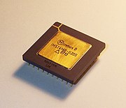
A transputer was a pioneering concurrent computing (parallel-processing) microprocessor design of the 1980s from INMOS, a British semiconductor company based in Bristol. [1]
For some time in the late 1980s many considered the transputer to be the next great design for the future of computing. While ultimately a commercial failure, the transputer architecture was highly influential in provoking new ideas in computer architecture, several of which have re-emerged in different forms in modern systems.
Contents |
[edit] Background
In the early 1980s, it appeared that conventional CPUs were reaching their performance limits. Up to that time, the amount of circuitry designers could place on a chip was limited primarily by manufacturing issues. But with continued improvements in the "fabbing" process (fabricating), this restriction vanished and soon the problem became that the chips could hold more circuitry than the designers knew how to use. Soon the traditional CISC designs were reaching a performance plateau, and it wasn't clear it could be overcome.
It seemed that the only way forward was to increase the use of parallelism, the use of several CPUs that would work together to solve several tasks at the same time. This depended on the machines in question being able to run several tasks at once, a process known as multitasking. This had generally been too difficult for previous CPU designs to handle, but more recent designs were able to accomplish it effectively. It was clear that in the future this would be a feature of all operating systems.
A side effect of most multitasking design is that it often also allows the processes to be run on physically different CPUs, in which case it is known as multiprocessing. A low-cost CPU built with multiprocessing in mind could allow the speed of a machine to be increased by adding more CPUs, potentially far more cheaply than by using a single faster CPU design.
[edit] Design
The transputer (transistor computer) was the first general purpose microprocessor designed specifically to be used in parallel computing systems. The goal was to produce a family of chips ranging in power and cost that could be wired together to form a complete computer. The name was selected to indicate the role the individual transputers would play: numbers of them would be used as basic building blocks, just as transistors had earlier.
Originally the plan was to make the transputer cost only a few dollars per unit. INMOS saw them being used for practically everything, from operating as the main CPU for a computer to acting as a channel controller for disk drives in the same machine. Spare cycles on any of these transputers could be used for other tasks, greatly increasing the overall performance of the machines.
Even a single transputer would have all the circuitry needed to work by itself, a feature more commonly associated with microcontrollers. The intention was to allow transputers to be connected together as easily as possible, without the requirement for a complex bus (or motherboard). Power and a simple clock signal had to be supplied, but little else: RAM, a RAM controller, bus support and even an RTOS were all built in.
[edit] Links
The basic design of the transputer included serial links that allowed it to communicate with up to four other transputers, each at 5, 10 or 20 Mbit/s – which was very fast for the 1980s. Any number of transputers could be connected together over even longish links (tens of metres) to form a single computing "farm". A hypothetical desktop machine might have two of the "low end" transputers handling I/O tasks on some of their serial lines (hooked up to appropriate hardware) while they talked to one of their larger cousins acting as a CPU on another.
There were limits to the size of a system that could be built in this fashion. Since each transputer was linked to another in a fixed point-to-point layout, sending messages to a more distant transputer required the messages to be relayed by each chip on the line. This introduced a delay with every "hop" over a link, leading to long delays on large nets. To solve this problem INMOS also provided a zero-delay switch that connected up to 32 transputers (or switches) into even larger networks.
[edit] Booting
Transputers could be booted over the network links (as opposed to the memory as in most machines) so a single transputer could start up the entire network. There was a pin called BootFromROM that when asserted caused the transputer to start two bytes from the top of memory (sufficient for up to a 256 byte backward jump, usually out of ROM). When this pin was not asserted, the first byte that arrived down any link was the length of a bootstrap to be downloaded, which was placed in low memory and run. The 'special' lengths of 0 and 1 were reserved for 'peek' and 'poke' - allowing inspection and changing of RAM in an unbooted transputer. After a peek (which required an address) or a poke (which took a word address, and a word of data - 16 or 32 bit depending on the basic word width of the transputer variant) the transputer would return to waiting for a bootstrap.
[edit] Scheduler
Supporting the links was additional circuitry that handled scheduling of the traffic over them. Processes waiting on communications would automatically pause while the networking circuitry finished its reads or writes. Other processes running on the transputer would then be given that processing time. It included two priority levels to improve real-time and multiprocessor operation. The same logical system was used to communicate between programs running on a single transputer, implemented as "virtual network links" in memory. So programs asking for any input or output automatically paused while the operation completed, a task that normally required the operating system to handle as the arbiter of hardware. Operating systems on the transputer did not have to handle scheduling: in fact, one could consider the chip itself to have an OS inside it.
To include all this functionality on a single chip, the transputer's core logic was simpler than most CPUs. While some have called it a RISC due to its rather spare nature (and because that was a desirable marketing buzzword at the time), it was heavily microcoded, had a limited register set, and complex memory-to-memory instructions, all of which place it firmly in the CISC camp. Unlike register-heavy load-store RISC CPUs, the transputer had only three data registers, which behaved as a stack. In addition a Workspace Pointer pointed to a conventional memory stack, easily accessible via the Load Local and Store Local instructions. This allowed for very fast context switching by simply changing the workspace pointer to the memory used by another process (a technique used in a number of contemporary designs). The three register stack contents were not preserved past certain instructions, like Jump, when the transputer could do a context switch.
[edit] Instruction set
The transputer instruction set comprised 8-bit instructions divided into opcode and operand nibbles. The "upper" nibble contained the 16 possible primary instruction codes, making it one of the very few commercialized minimal instruction set computers. The "lower" nibble contained the single immediate constant operand, commonly used as an offset relative to the Workspace (memory stack) pointer. Two prefix instructions allowed construction of larger constants by prepending their lower nibbles to the operands of following instructions. Additional instructions were supported via the Operate (Opr) instruction code, which decoded the constant operand as an extended zero-operand opcode, providing for almost endless and easy instruction set expansion as newer implementations of the transputer were introduced.
The 16 'primary' one-operand instructions were :-
| Mnemonic | Description |
| J | Jump — add immediate operand to instruction pointer. |
| LDLP | Load Local Pointer — load a Workspace-relative pointer onto the top of the register stack |
| PFIX | Prefix — general way to increase lower nibble of following primary instruction |
| LDNL | Load non-local — load a value offset from address at top of stack |
| LDC | Load constant — load constant operand onto the top of the register stack |
| LDNLP | Load Non-local pointer — Load address, offset from top of stack |
| NFIX | Negative prefix — general way to negate (and possibly increase) lower nibble |
| LDL | Load Local — load value offset from Workspace |
| ADC | Add Constant — add constant operand to top of register stack |
| CALL | Subroutine call — push instruction pointer and jump |
| CJ | Conditional jump — depending on value at top of register stack |
| AJW | Adjust workspace — add operand to workspace pointer |
| EQC | Equals constant — test if top of register stack equals constant operand |
| STL | Store local - store at constant offset from workspace |
| STNL | Store non-local - store at address offset from top of stack |
| OPR | Operate - general way to extend instruction set |
All these instructions take a constant, representing an offset or an arithmetic constant. If this constant was less than 16, all these instructions coded to a single byte.
The first 16 'secondary' zero-operand instructions (using the OPR primary instruction) were :-
| Mnemonic | Description |
| REV | Reverse — swap two top items of register stack |
| LB | Load byte |
| BSUB | Byte subscript |
| ENDP | End process |
| DIFF | Difference |
| ADD | Add |
| GCALL | General Call - swap top of stack and instruction pointer |
| IN | Input — receive message |
| PROD | Product |
| GT | Greater Than — the only comparison instruction |
| WSUB | Word subscript |
| OUT | Output — send message |
| SUB | Subtract |
| STARTP | Start Process |
| OUTBYTE | Output Byte — send single-byte message |
| OUTWORD | Output word — send single-word message |
[edit] TRAMs
To provide an easy means of prototyping, constructing and configuring multiple-transputer systems, INMOS introduced the TRAM (TRAnsputer Module) standard in 1987. A TRAM was essentially a building block daughterboard comprising a transputer and, optionally, external memory and/or peripheral devices, with simple standardised connectors providing power, transputer links, clock and system signals. Various sizes of TRAM were defined, from the basic Size 1 TRAM (3.66 in by 1.05 in) up to Size 8 (3.66 in by 8.75 in). INMOS produced a range of TRAM motherboards for various host buses such as ISA, MicroChannel or VMEbus.
[edit] Software
Transputers were intended to be programmed using the occam programming language, based on the CSP process calculus. In fact it is fair to say that the transputer was built specifically to run occam, even more so than contemporary CISC designs were built to run languages like Pascal or C. Occam supported concurrency and channel-based inter-process or inter-processor communication as a fundamental part of the language. With the parallelism and communications built into the chip and the language interacting with it directly, writing code for things like device controllers became a triviality – even the most basic code could watch the serial ports for I/O, and would automatically sleep when there was no data.
The initial occam development environment for the transputer was the INMOS D700 Transputer Development System (TDS). This was an unorthodox integrated development environment incorporating an editor, compiler, linker and (post-mortem) debugger. The TDS was itself a transputer application written in occam. The TDS text editor was notable in that it was a folding editor, allowing blocks of code to be hidden and revealed, to make the structure of the code more apparent. Unfortunately, the combination of an unfamiliar programming language and equally unfamiliar development environment did nothing for the early popularity of the transputer. Later, INMOS would release more conventional occam cross-compilers, the occam 2 Toolsets.
Implementations of more mainstream programming languages, such as C, FORTRAN, Ada and Pascal were also later released by both INMOS and third-party vendors. These usually included language extensions or libraries providing, in a less elegant way, occam-like concurrency and channel-based communication.
The transputer's lack of support for virtual memory inhibited the porting of mainstream variants of the UNIX operating system, though ports of UNIX-like operating systems (such as Minix and Idris from Whitesmiths) were produced. An advanced UNIX-like distributed operating system, HeliOS, was also designed specifically for multi-transputer systems by Perihelion Software.
[edit] Implementations
The first transputers were announced in 1983 and released in 1984.
In keeping with their role as microcontroller-like devices, they included on-board RAM and a built-in RAM controller which enabled more memory to be added without any additional hardware. Unlike other designs, transputers did not include I/O lines: these were to be added with hardware attached to the existing serial links. There was one 'Event' line, similar to a conventional processor's interrupt line. Treated as a channel, a program could 'input' from the event channel, and proceed only after the event line was asserted.
All transputers ran from an external 5 MHz clock input; this was multiplied to provide the processor clock.
The transputer did not include an MMU or a virtual memory system.
Transputer variants (excepting the cancelled T9000) can be categorised into three groups: the 16-bit T2 series, the 32-bit T4 series and the 32-bit T8 series with 64-bit IEEE 754 floating-point support.
[edit] T2: 16-bit
The prototype 16-bit transputer was the S43, which lacked the scheduler and DMA-controlled block transfer on the links. At launch, the T212 and M212 (the latter with an on-board disk controller) were the 16-bit offerings. The T212 was available in 17.5 and 20 MHz processor clock speed ratings. The T212 was superseded by the T222, with on-chip RAM expanded from 2 kB to 4kB, and, later, the T225. This added debugging breakpoint support (by extending the instruction J 0) plus some extra instructions from the T800 instruction set. Both the T222 and T225 ran at 20 MHz.
[edit] T4: 32-bit
At launch, the T414 was the 32-bit offering. Originally, the first 32-bit variant was to be the T424, but fabrication difficulties meant that this was redesigned as the T414 with 2 kB on-board RAM instead of the intended 4 kB. The T414 was available in 15 and 20 MHz varieties. The RAM was later reinstated to 4 kB on the T425 (in 20, 25 and 30 MHz varieties), which also added the J 0 breakpoint support and extra T800 instructions. The T400, released in September 1989, was a low-cost 20 MHz T425 derivative with 2 kB and two instead of four links, intended for the embedded systems market.
[edit] T8: floating point
The second-generation T800 transputer, introduced in 1987, included a 64-bit floating point unit and three additional registers for floating point use, in addition to an extended instruction set. It also had 4 kB of on-board RAM and was available in 20 or 25 MHz versions. Breakpoint support was added in the later T801 and T805, the former featuring separate address and data buses to improve performance. The T805 was also later available as a 30 MHz part.
An enhanced T810 was planned, which would have had more RAM, more and faster links, extra instructions and improved microcode, but this was cancelled around 1990.
INMOS also produced a variety of support chips for the transputer processors, such as the C004 32-way link switch and the C012 "link adapter" which allowed transputer links to be interfaced to an 8-bit data bus.
[edit] Markets
While the transputer was simple but powerful compared to many contemporary designs, it never came close to meeting its goal of being used universally in both CPU and microcontroller roles. In the microcontroller realm, the market was dominated by 8-bit machines where cost was the only serious consideration. Here, even the T2s were too powerful and expensive for most users.
In the computer desktop/workstation world, the transputer was fairly fast (operating at about 10 MIPS at 20 MHz). This was excellent performance for the early 1980s, but by the time the FPU-equipped T800 was shipping, other RISC designs had surpassed it. This could have been mitigated to a large extent if machines had used multiple transputers as planned, but T800s cost about $400 each when introduced, which meant a poor price/performance ratio. Few transputer-based workstation systems were designed; the most notable probably being the Atari Transputer Workstation.
The transputer was more successful in the field of massively parallel computing, where several vendors produced transputer-based systems in the late 1980s. These included Meiko (founded by ex-INMOS employees), Floating Point Systems, Parsytec and Parsys. Several British academic institutions founded research activities in the application of transputer-based parallel systems, including Bristol Polytechnic's Bristol Transputer Centre and the University of Edinburgh's Edinburgh Concurrent Supercomputer Project.
The parallel processing capabilities of the transputer were put to use commercially for image processing by the worlds largest printing company, RR Donnelley & Sons, in the early 1990s. The ability to quickly transform digital images in preparation for print gave RR Donnelley a significant edge over their competitors. This development was led by Michael Bengtson in the RR Donnelley Technology Center. Within a few years, the processing capability of even desktop computers pushed aside the need for custom multi-processing systems for RR Donnelley.[citation needed]
[edit] T9000
INMOS improved on the performance of the T8 series transputers with the introduction of the T9000 (code-named H1 during development). The T9000 shared most features with the T800, but moved several pieces of the design into hardware and added several features for superscalar support. Unlike the earlier models, the T9000 had a true 16 kB high-speed cache (using random-replacement) instead of RAM, but also allowed it to be used as memory and included MMU-like functionality to handle all of this (known as the PMI). For additional speed the T9000 cached the top 32 locations of the stack, instead of three as in earlier versions.
The T9000 used a five stage pipeline for even more speed. An interesting addition was the grouper which would collect instructions out of the cache and group them into larger packages of 4 bytes to feed the pipeline faster. Groups then completed in a single cycle, as if they were single larger instructions working on a faster CPU.
The link system was upgraded to a new 100 MHz mode, but unlike the previous systems the links were no longer downwardly compatible. This new packet-based link protocol was called DS-Link and later formed the basis of the IEEE 1355 serial interconnect standard. The T9000 also added link routing hardware called the VCP (Virtual Channel Processor) which changed the links from point-to-point to a true network, allowing for the creation of any number of virtual channels on the links. This meant programs no longer had to be aware of the physical layout of the connections. A range of DS-Link support chips were also developed, including the C104 32-way crossbar switch, and the C101 link adapter.
Long delays in the T9000's development meant that the faster load-store designs were already outperforming it by the time it was to be released. In fact it consistently failed to reach its own performance goal of beating by a factor of ten the T800: when the project was finally cancelled it was still achieving only about 36 MIPS at 50 MHz. The production delays gave rise to the quip that the best host architecture for a T9000 was an overhead projector.
This was too much for INMOS, who didn't have the funding needed to continue development. By this time, the company had been sold to SGS-Thomson (now STMicroelectronics), whose focus was the embedded systems market, and eventually the T9000 project was abandoned. However, a comprehensively redesigned 32-bit transputer intended for embedded applications, the ST20 series, was later produced, utilising some technology developed for the T9000. The ST20 core was incorporated into chipsets for set-top box and GPS applications.
[edit] Comparison with modern technology
|
|
This section is written like a personal reflection or essay and may require cleanup. Please help improve it by rewriting it in an encyclopedic style. (February 2009) |
Ironically it was largely through additional internal parallelism that conventional CPU designs got faster. Instead of using an explicit thread-level system like the transputer, CPU designs became parallel implicitly at the instruction level, looking at the code being run and then distributing instructions that don't affect each-others' results across a number of internal arithmetic units within the CPU core. This form of parallelism, known as superscalar, has proved more suitable to general purpose computing. Most critically, it and speculative execution delivered a tangible performance increase to existing code. By speeding up existing applications, the classic 'single CPU' microprocessor managed to outrun parallel systems such as the transputer, whose performance benefits only showed up in massive-multiprocessor installations. The mainstream programming languages of the time - Pascal, Fortran, C and later C++ - lacked any intrinsic parallelisation, so this single-CPU parallelism delivered a speedup without the need to rewrite the application using immature technologies.
Nevertheless, the model of multiple cheap, cooperating processors can be found in the proliferating cluster computing systems that have dominated supercomputer design in the 21st century. Unlike in the proposed transputer architecture, the processing units in these systems are typically similar to conventional servers. They possess CPUs with an internal superscalar architecture, access to substantial amounts of memory and often disk storage, and conventional operating systems and network interfaces. The software architecture used to marshal the cooperating software processes across the loosely coupled processors in these systems is typically far more heavyweight than that implemented in the transputer architecture.
The fundamental problem that the transputer was trying to solve, however, did not go away with the transputer's failure. The problem lay mostly dormant for over 20 more years -- during which time transistor counts doubled again and again -- but microprocessor designers finally did run out of purposes to which employ the physical resources available. Moreover, the solutions on which the industry has settled are little different in essence from those proposed by INMOS.
Today (2007), the same Intel Core 2 die, with little modification, is sought after to power everything from 2-pound notebooks to multiton supercomputers. The trend toward consolidating components, especially network interfaces, into the commodity CPU itself is also well under way and is forecast to become mainstream soon. Moreover, much excitement centers around more specialized System-on-a-Chip designs that, like the transputer, are almost entirely self-contained. In fact, the most powerful supercomputers in the world, based on designs from Columbia University and built as IBM Blue Gene, are nothing less or more than real-world incarnations of the transputer dream. They are vast assemblies of identical, relatively low-performance SoC chips.
Recent trends have also tried to solve the transistor dilemma in ways that would have been too anachronistic even for INMOS. Beside adding components to the CPU die and placing multiple dies in one system, modern processors increasingly place multiple cores in one die. While the transputer struggled to fit even one core into its transistor budget, designers, working with a 1000 fold more transistors, now typically place several.
[edit] See also
- David May, transputer architect
- Atari Transputer Workstation
- IEEE 1355 data interconnect standard derived from T9000 DS-links
- Meiko Computing Surface
- iWarp
- Ease programming language
[edit] References
- ^ Allen Kent, James G. Williams (eds.) (1998) "Encyclopedia of Computer Science and Technology", ISBN 0824722922, "The Transputer Family of Products", by Hamid R. Arabnia
[edit] External links
| Wikimedia Commons has media related to: Transputer |
- The Transputer Archive
- John Catsoulis' article on Transputer Hardware
- Transputer
- The Transputer FAQ
- Ram Meenakshisundaram's Transputer Home Page
- WoTUG A group applying the principles of transputers (e.g., CSP) in other environments.
- Transputer emulator - It emulates a single T414 transputer (i.e. no FPU, no blitting instructions) and supplies the file and terminal I/O services that were usually supplied by the host computer system.
- Transputers can be fun.
- The Transterpreter virtual machine. - A portable runtime for occam-pi and other languages based on the transputer bytecode.
- The Kent Retargettable occam compiler. - The occam-pi compiler.
- transputer.net. - Documents and more about transputer.
|
||||||||||||||||||||||||||||||||

