Phase-locked loop
From Wikipedia, the free encyclopedia
for the Rubik's Cube Permutation of Last Layer, see Fridrich Method;
for the spinal ligament, see Posterior longitudinal ligament.A phase-locked loop or phase lock loop (PLL) is a control system that generates a signal that has a fixed relation to the phase of a "reference" signal. A phase-locked loop circuit responds to both the frequency and the phase of the input signals, automatically raising or lowering the frequency of a controlled oscillator until it is matched to the reference in both frequency and phase. A phase-locked loop is an example of a control system using negative feedback.
In simpler terms, a PLL compares the frequencies of two signals and produces an error signal which is proportional to the difference between the input frequencies. The error signal is then low-pass filtered and used to drive a voltage-controlled oscillator (VCO) which creates an output frequency. The output frequency is fed through a frequency divider back to the input of the system, producing a negative feedback loop. If the output frequency drifts, the error signal will increase, driving the frequency in the opposite direction so as to reduce the error. Thus the output is locked to the frequency at the other input. This input is called the reference and is often derived from a crystal oscillator, which is very stable in frequency.

Phase-locked loops are widely used in radio, telecommunications, computers and other electronic applications. They may generate stable frequencies, recover a signal from a noisy communication channel, or distribute clock timing pulses in digital logic designs such as microprocessors. Since a single integrated circuit can provide a complete phase-locked-loop building block, the technique is widely used in modern electronic devices, with output frequencies from a fraction of a cycle per second up to many gigahertz.
Contents |
[edit] Analogy
Tuning a string on a guitar can be compared to the operation of a phase-locked loop. Using a tuning fork or pitchpipe to provide a reference frequency, the tension of the string is adjusted up or down until the beat frequency is inaudible. This indicates that the tuning fork and guitar are vibrating at the same frequency. If we imagine the guitar could be tuned perfectly to the reference tuning fork frequency, and maintained there, the guitar string would be said to be in phase-lock with the fork.
[edit] History
Earliest research towards what became known as the phase-locked loop goes back to 1932, when British researchers developed an alternative to Edwin Armstrong's superheterodyne receiver, the Homodyne or direct-conversion receiver. In the homodyne or synchrodyne system, a local oscillator was tuned to the desired input frequency and multiplied with the input signal. The resulting output signal included the original audio modulation information. The intent was to develop an alternative receiver circuit that required fewer tuned circuits than the superheterodyne receiver. Since the local oscillator would rapidly drift in frequency, an automatic correction signal was applied to the oscillator, maintaining it in the same phase and frequency as the desired signal. The technique was described in 1932, in a paper by Henri de Bellescize, in the French journal Onde Electrique.[1]
In analog television receivers since at least the late 1930s, phase-locked-loop horizontal and vertical sweep circuits are locked to synchronization pulses in the broadcast signal.[2]
When Signetics introduced a line of monolithic integrated circuits that were complete phase-locked loop systems on a chip in 1969,[3] applications for the technique multiplied. A few years later RCA introduced the "CD4046" CMOS Micropower Phase-Locked Loop, which became a popular integrated circuit.
[edit] Structure and function
Phase-locked loop mechanisms may be implemented as either analog or digital circuits. Both implementations use the same basic structure.

Both analog and digital PLL circuits include three basic elements:
- a phase detector,
- a variable electronic oscillator, and
- a feedback path (which often includes a frequency divider).
[edit] Digital phase-locked loop (DPLL)
A digital phase-locked loop operates similarly to an analog phase-locked loop, but is implemented entirely using digital circuits. In place of a voltage-controlled oscillator (VCO), a DPLL uses local reference clock and an variable dividing counter under digital control to create the equivalent oscillator function.
DPLLs are easier to design and implement, and are less sensitive to voltage noise than analog PLLs, however they typically suffer from higher phase noise due to the quantization error of using a non-analog oscillator. For this reason digital phase locked loops are not well-suited to synthesizing higher frequencies or handling high frequency reference signals. DPLLs are sometimes used for data recovery.
[edit] Analog phase-locked loop
[edit] Basic design

Analog phase locked loops are generally built of a phase detector, low pass filter and voltage-controlled oscillator (VCO) placed in a negative feedback closed-loop configuration. There may be a frequency divider in the feedback path or in the reference path, or both, in order to make the PLL's output signal frequency an integer multiple of the reference. A non integer multiple of the reference frequency can be created by replacing the simple divide-by-N counter in the feedback path with a programmable pulse swallowing counter. This technique is usually referred to as a fractional-N synthesizer or fractional-N PLL.
The oscillator generates a periodic output signal. Assume that initially the oscillator is at nearly the same frequency as the reference signal. Then, if the phase from the oscillator falls behind that of the reference, the phase detector changes the control voltage of the oscillator, so that it speeds up. Likewise, if the phase creeps ahead of the reference, the phase detector changes the control voltage to slow down the oscillator. A low-pass filter smooths out abrupt changes in the control voltage; it can be demonstrated that some filtering is required for a stable system. Since initially the oscillator may be far from the reference frequency, practical phase detectors may also respond to frequency differences, so as to increase the lock-in range of allowable inputs.
Depending on the application, either the output of the controlled oscillator, or the control signal to the oscillator, provides the useful output of the PLL system.
[edit] Elements
[edit] Phase detector
The two inputs of the phase detector (PD) are the reference input (Fi) and the feedback from the voltage controlled oscillator (VCO). The PD output controls the VCO such that the phase difference between the two inputs is held constant, making it a negative feedback system.
There are several types of phase detectors in two main categories of analog and digital.
[edit] Analog
The analog phase detector takes the form of an ideal frequency mixer. This device produces an output that is the product of the two instantaneous input voltages. The multiplication process produces the classical sum and difference frequencies of mixers, but when used as a phase detector, a Low-pass filter is required to attenuate the sum frequency. When the remaining difference frequency is low enough to pass through the filter with sufficient amplitude, it moves the VCO frequency closer to the reference frequency allowing the loop, after a transient period, to acquire lock. This process is called "capture" and the maximum frequency separation (between reference input and VCO) that allows lock is the "capture range". The loop is called "locked" when the VCO is on the same frequency as the reference and differs only in some amount of phase.
When the loop is locked, the sum and difference are still present, but the sum becomes a frequency twice that of the reference. The difference, which appears as the average value of the sum frequency, becomes, after the filter, a DC component proportional to the (cosine of the) phase difference. This then sets the VCO frequency.
The phase difference at the inputs, when in lock, is near 90 degrees for this type; the exact amount being determined by the loop gain. Though an additional integration can be added to bring it to 90, this is rarely required in simple loops.
The phase and amplitude characteristics of the low-pass filter are dominant factors in determining the capture range, lock time and transient performance of the loop.
Two common implementations are the double balanced diode mixer and the four-quadrant multiplier (which is also a double balanced mixer).
The presence of the sum frequency at the mixer output also adds complexity in applications where spectral purity of the VCO signal is important. This causes frequency modulation of the VCO at twice the reference frequency. The resulting unwanted (spurious) sidebands, also called "reference spurs" can dominate the filter requirements and reduce the capture range and lock time well below the requirements. In these applications the more complex digital phase detectors are used which do not have as severe a reference spur component on their output.
[edit] Digital
The simplest is an XOR gate. It compares well to the analog mixer in that it locks near a 90° phase difference and has a square-wave output at twice the reference frequency. The average value of this square wave is the DC component that sets the VCO frequency. The square-wave changes duty-cycle in proportion to the phase difference resulting, after the filter, in the VCO control voltage. It requires inputs that are symmetrical square waves, or nearly so. The remainder of its characteristics are very similar to the analog mixer for capture range, lock time, reference spurious and low-pass filter requirements.
A more complex digital PD uses a simple state machine to determine which of the two signals has a zero-crossing earlier or more often. This brings the PLL into lock even when it is off frequency and is known as a Phase Frequency Detector.
A PLL with a bang-bang charge pump phase detector supplies current pulses with fixed total charge, either positive or negative, to the capacitor acting as an integrator. A phase detector for a bang-bang charge pump must always have a dead band where the phases of the reference and feedback clocks are close enough that the detector fires either both or neither of the charge pumps, for no total effect. Bang-bang phase detectors are simple, but are associated with significant minimum peak-to-peak jitter, because once in lock the phase offset drifts inside the two extreme values of the dead band without triggering any corrections.
A proportional phase detector employs a charge pump that supplies charge amounts in proportion to the phase error detected. Some have dead bands and some do not. A dead band is an area where small changes in phase difference produce no correction to the VCO. Specifically, some designs produce both "up" and "down" control pulses even when the phase difference is zero. These pulses are small, nominally the same duration, and cause the charge pump to produce equal-charge positive and negative current pulses when the phase is perfectly matched. If the inputs are slightly mismatched, either the up or down pulse will contain slightly more charge than the other and the PLL will be able to correct the offset. PLLs with this kind of control system don't exhibit a dead band and typically have lower minimum peak-to-peak jitter that is determined by other limiting factors.
These types, having outputs consisting of very narrow pulses at lock, are very useful for applications requiring very low VCO spurious outputs. The narrow pulses contain very little energy and are easy to filter out of the VCO control voltage. This results in low VCO control line ripple and therefore low FM sidebands on the VCO.
It is frequently required to know when the loop is out of lock. The more complex digital phase-frequency detectors usually have an output that allows a reliable indication of an out of lock condition.
[edit] Oscillator types
Inductive oscillators (LC oscillators) are built of an LC "tank" circuit, which oscillates by charging and discharging a capacitor through an inductor. These oscillators are typically used when a tunable precision frequency source is necessary, such as with radio transmitters and receivers. Most LC oscillators use off-chip inductors. On-chip inductors suffer large resistive losses, so that the Q of the resulting tank circuit is generally less than 10. As processes have made larger numbers of metal layers available (allowing designers to distance the inductor metal layer from the resistive substrate), on-chip inductors have become more useful.
A voltage-controlled capacitor is one method of making an LC oscillator vary its frequency in response to a control voltage. Any reverse-biased semiconductor diode displays a measure of voltage-dependent capacitance and can be used to change the frequency of an oscillator by varying a control voltage applied to the diodes. Special-purpose variable capacitance varactor diodes are available with well-characterized wide-ranging values of capacitance. Such devices are very convenient in the manufacture of voltage-controlled oscillators (a voltage-controlled inductor would be in principle as useful, but such devices are unsatisfactory at the frequencies usually desired).
Crystal oscillators are piezoelectric quartz crystals that mechanically vibrate between two slightly different shapes. Crystals have very high Q, and can only be tuned within a very small range of frequencies. Crystal oscillators are typically used as the frequency reference for PLLs, and can be found in nearly every consumer electronic device. Because the crystal is an off-chip component, it adds some cost and complexity to the system design, but the crystal itself is generally quite inexpensive.
- Surface acoustic wave devices (SAWs) are a kind of crystal oscillator, but achieve much higher frequencies by establishing standing waves on the surface of the quartz crystal. These are more expensive than crystal oscillators, and are used in more specialized applications which require a direct and very accurate high frequency reference, for example, in cellular telephones.
For a PLL built into a microprocessor chip, ring oscillators can be used as voltage-controlled oscillators-a free running multivibrator (VCOs). They are built of a ring of active delay stages. Generally the ring has an odd number of inverting stages, so that there is no single stable state for the internal ring voltages. Instead, a single transition propagates endlessly around the ring. The frequency is controlled by varying either the supply voltage or the capacitive loading on each stage. VCOs generally have the lowest Q of the used oscillators, and so suffer more jitter than the other types. The jitter can be made low enough for many applications (such as driving an ASIC), in which case VCOs enjoy the advantages of having no off-chip components (expensive) or on-chip inductors (low yields on generic CMOS processes). These oscillators also have larger tuning ranges than the other kinds, which improves yield and is sometimes a feature of the end product (for instance, the dot clock on a graphics card which drives a wide range of monitors).
[edit] Feedback path and optional divider
Most PLLs also include a divider between the oscillator and the feedback input to the phase detector to produce a frequency synthesizer. A programmable divider is particularly useful in radio transmitter applications, since a large number of transmit frequencies can be produced from a single stable, accurate, but expensive, quartz crystal–controlled reference oscillator.
Some PLLs also include a divider between the reference clock and the reference input to the phase detector. If this divider divides by M, it allows the VCO to multiply the reference frequency by N / M. It might seem simpler to just feed the PLL a lower frequency, but in some cases the reference frequency may be constrained by other issues, and then the reference divider is useful. Frequency multiplication in a sense can also be attained by locking the PLL to the 'N'th harmonic of the signal.
[edit] Equations
The equations governing a phase-locked loop with an analog multiplier as the phase detector may be derived as follows. Let the input to the phase detector be xc(t) and the output of the voltage-controlled oscillator (VCO) is xr(t) with frequency ωr(t), then the output of the phase detector xm(t) is given by

the VCO frequency may be written as a function of the VCO input y(t) as

where gv is the sensitivity of the VCO and is expressed in Hz / V.
Hence the VCO output takes the form

where

The loop filter receives this signal as input and produces an output
- xf(t) = Ffilter(xm(t))
where FFilter is the operator representing the loop filter transformation.
When the loop is closed, the output from the loop filter becomes the input to the VCO thus
- y(t) = xf(t) = Ffilter(xm(t))
We can deduce how the PLL reacts to a sinusoidal input signal:
- xc(t) = Acsin(ωct).
The output of the phase detector then is:

This can be rewritten into sum and difference components using trigonometric identities:

As an approximation to the behaviour of the loop filter we may consider only the difference frequency being passed with no phase change, which enables us to derive a small-signal model of the phase-locked loop. If we can make  , then the
  can be approximated by its argument resulting in:
  . The phase-locked loop is said to be locked if this is the case.[4]
[edit] Control system analysis
Phase locked loops can also be analyzed as control systems by applying the Laplace transform. The loop response can be written as:

Where
- θo is the output phase in radians
- θi is the input phase in radians
- Kp is the phase detector gain in volts per radian
- Kv is the VCO gain in radians per volt-second
- F(s) is the loop filter transfer function (dimensionless)
The loop characteristics can be controlled by inserting different types of loop filters. The simplest filter is a one-pole RC circuit. The loop transfer function in this case is:

The loop response becomes:

This is the form of a classic harmonic oscillator. The denominator can be related to that of a second order system:

Where
- ζ is the damping factor
- ωn is the natural frequency of the loop
For the one-pole RC filter,
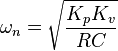

The loop natural frequency is a measure of the response time of the loop, and the damping factor is a measure of the overshoot and ringing. Ideally, the natural frequency should be high and the damping factor should be near 0.707 (critical damping). With a single pole filter, it is not possible to control the loop frequency and damping factor independently. For the case of critical damping,


A slightly more effective filter, the lag-lead filter includes one pole and one zero. This can be realized with two resistors and one capacitor. The transfer function for this filter is

This filter has two time constants
- τ1 = C(R1 + R2)
- τ2 = CR2
Substituting above yields the following natural frequency and damping factor


The loop filter components can be calculated independently for a given natural frequency and damping factor


Real world loop filter design can be much more complex eg using higher order filters to reduce various types or source of phase noise. (See the D Banerjee ref below)
[edit] Applications
Phase-locked loops are widely used for synchronization purposes; in space communications for coherent carrier tracking and threshold extension, bit synchronization, and symbol synchronization. Phase-locked loops can also be used to demodulate frequency-modulated signals. In radio transmitters, a PLL is used to synthesize new frequencies which are a multiple of a reference frequency, with the same stability as the reference frequency.
[edit] Clock recovery
Some data streams, especially high-speed serial data streams (such as the raw stream of data from the magnetic head of a disk drive), are sent without an accompanying clock. The receiver generates a clock from an approximate frequency reference, and then phase-aligns to the transitions in the data stream with a PLL. This process is referred to as clock recovery. In order for this scheme to work, the data stream must have a transition frequently enough to correct any drift in the PLL's oscillator. Typically, some sort of redundant encoding is used; 8B10B is very common.
[edit] Deskewing
If a clock is sent in parallel with data, that clock can be used to sample the data. Because the clock must be received and amplified before it can drive the flip-flops which sample the data, there will be a finite, and process-, temperature-, and voltage-dependent delay between the detected clock edge and the received data window. This delay limits the frequency at which data can be sent. One way of eliminating this delay is to include a deskew PLL on the receive side, so that the clock at each data flip-flop is phase-matched to the received clock. In that type of application, a special form of a PLL called a Delay-Locked Loop (DLL) is frequently used.[5]
[edit] Clock generation
Many electronic systems include processors of various sorts that operate at hundreds of megahertz. Typically, the clocks supplied to these processors come from clock generator PLLs, which multiply a lower-frequency reference clock (usually 50 or 100 MHz) up to the operating frequency of the processor. The multiplication factor can be quite large in cases where the operating frequency is multiple gigahertz and the reference crystal is just tens or hundreds of megahertz.
[edit] Spread spectrum
All electronic systems emit some unwanted radio frequency energy. Various regulatory agencies (such as the FCC in the United States) put limits on the emitted energy and any interference caused by it. The emitted noise generally appears at sharp spectral peaks (usually at the operating frequency of the device, and a few harmonics). A system designer can use a spread-spectrum PLL to reduce interference with high-Q receivers by spreading the energy over a larger portion of the spectrum. For example, by changing the operating frequency up and down by a small amount (about 1%), a device running at hundreds of megahertz can spread its interference evenly over a few megahertz of spectrum, which drastically reduces the amount of noise seen by FM receivers which have a bandwidth of tens of kilohertz.
[edit] Clock distribution

Typically, the reference clock enters the chip and drives a phase locked loop (PLL), which then drives the system's clock distribution. The clock distribution is usually balanced so that the clock arrives at every endpoint simultaneously. One of those endpoints is the PLL's feedback input. The function of the PLL is to compare the distributed clock to the incoming reference clock, and vary the phase and frequency of its output until the reference and feedback clocks are phase and frequency matched. From a control theory perspective, the PLL is a special case of the Kalman filter.
PLLs are ubiquitous -- they tune clocks in systems several feet across, as well as clocks in small portions of individual chips. Sometimes the reference clock may not actually be a pure clock at all, but rather a data stream with enough transitions that the PLL is able to recover a regular clock from that stream. Sometimes the reference clock is the same frequency as the clock driven through the clock distribution, other times the distributed clock may be some rational multiple of the reference.
[edit] Jitter and noise reduction
One desirable property of all PLLs is that the reference and feedback clock edges be brought into very close alignment. The average difference in time between the phases of the two signals when the PLL has achieved lock is called the static phase offset (also called the steady-state phase error). The variance between these phases is called tracking jitter. Ideally, the static phase offset should be zero, and the tracking jitter should be as low as possible.
Phase noise is another type of jitter observed in PLLs, and is mostly caused by the amplifier elements used in the circuit. Some technologies are known to perform better than others in this regard. The best digital PLLs are constructed with emitter-coupled logic (ECL) elements, at the expense of high power consumption. To keep phase noise low in PLL circuits, it is best to avoid saturating logic families such as transistor-transistor logic (TTL) or CMOS.
Another desirable property of all PLLs is that the phase and frequency of the generated clock be unaffected by rapid changes in the voltages of the power and ground supply lines, as well as the voltage of the substrate on which the PLL circuits are fabricated. This is called supply and substrate noise rejection. The higher the noise rejection, the better.
To further improve the phase noise of the output oscillation, an injection locked oscillator can be employed following the voltage controlled oscillator in the PLL.
[edit] Frequency Synthesis
In digital wireless communication systems (GSM, CDMA etc), PLL's are used to provide the Local Oscillator (LO) for up-conversion during transmission, and down-conversion during reception. In most cellular handsets this function has been largely integrated into a single integrated circuit to reduce the cost and size of the handset. However due to the high performance required of base station terminals, the transmission and reception circuits are built with discrete components to achieve the levels of performance required. GSM LO modules are typically built with a Frequency Synthesizer integrated circuit, and discrete resonator VCO's.
Frequency Synthesizer manufacturers include Analog Devices[6], National Semiconductor and Texas Instruments. VCO manufacturers include Sirenza, Z-Communications, Inc. (Z-COMM)
Other applications include:
- Demodulation of both FM and AM signals
- Recovery of small signals that otherwise would be lost in noise (lock-in amplifier)
- Recovery of clock timing information from a data stream such as from a disk drive
- Clock multipliers in microprocessors that allow internal processor elements to run faster than external connections, while maintaining precise timing relationships
- DTMF decoders, modems, and other tone decoders, for remote control and telecommunications
[edit] See also
- Control theory
- Numerically-controlled oscillator - also known as a Digitally-controlled oscillator (DCO). These are instances of direct synthesizers, which synthesize a digital waveform using a lookup table driven by a counter that is incremented at the reference frequency.
- Costas loop
- Kalman filter
- Direct conversion receiver
- Circle map - a simple mathematical model of the phase-locked loop showing both mode-locking and chaotic behaviour.
- Carrier recovery
[edit] References
- ^ Notes for a University of Guelph course describing the PLL and early history, including an IC PLL tutorial
- ^ National Television Systems Committee Video Display Signal
- ^ A. B. Grebene, H. R. Camenzind, “Phase Locking As A New Approach For Tuned Integrated Circuits”, ISSCC Digest of Technical Papers, pp. 100-101, Feb. 1969.
- ^ This article contains material from the Federal Standard 1037C (in support of MIL-STD-188), which, as a work of the United States Government, is in the public domain.
- ^ M Horowitz, C. Yang, S. Sidiropoulos (1998-01-01). "High-speed electrical signaling: overview and limitations". IEEE Micro. http://www-vlsi.stanford.edu/papers/mh_micro_98.pdf.
- ^ List of PLL Synthesizers/VCOs from Analog Devices
- H. de Bellescise, La réception Synchrone, Onde Electrique, volume 11, 1932.
- William F. Egan, Phase-Lock Basics, John Wiley & Sons, 1998 (provides useful Matlab scripts for simulation)
- William F. Egan, Frequency Synthesis by Phase Lock (2nd ed.), John Wiley and Sons, 2000 (provides useful Matlab scripts for simulation)
- Dan H. Wolaver, Phase-Locked Loop Circuit Design, Prentice Hall, 1991, ISBN-10: 0136627439
- Richard C. Dorf, The Electrical Engineering Handbook, CRC Press, Boca Raton 1993 ISBN 0-8493-0185-8
- R. E. Best, Phase-locked Loops: Design, Simulation and Applications, McGraw-Hill 2003, ISBN 0-07-141201-8
- Floyd M. Gardner, Phaselock Techniques
- J. Klapper and J. T. Frankle, "Phase-Locked and Frequency-Feedback Systems", Academic Press 1972 (FM Demodulation)
- Predicting the Phase Noise and Jitter of PLL-Based Frequency Synthesizers
- Build a 1.5-V 2.4-GHz CMOS PLL — an article on designing a standard PLL IC for Bluetooth applications.
- PLL Performance, Simulation and Design Handbook by Dean Banerjee from National Semiconductor (PDF version).
| Wikimedia Commons has media related to: Phase-locked loops |

