Dynamic random access memory
From Wikipedia, the free encyclopedia
| Computer memory types |
| Volatile |
| Non-volatile |
Dynamic random access memory (DRAM) is a type of random access memory that stores each bit of data in a separate capacitor within an integrated circuit. Since real capacitors leak charge, the information eventually fades unless the capacitor charge is refreshed periodically. Because of this refresh requirement, it is a dynamic memory as opposed to SRAM and other static memory.
The advantage of DRAM is its structural simplicity: only one transistor and a capacitor are required per bit, compared to six transistors in SRAM. This allows DRAM to reach very high density. Unlike Flash memory, it is volatile memory (cf. non-volatile memory), since it loses its data when the power supply is removed.
[edit] History
| This section requires expansion. |

In 1964, Arnold Farber and Eugene Schlig working for IBM created a memory cell that was hard wired; using a transistor gate and tunnel diode latch, they later replaced the latch with two transistors and two resistors, which became known as the Farber-Schlig cell. In 1965, Benjamin Agusta and his team working for IBM managed to create a 16-bit silicon chip memory cell based on the Farber-Schlig cell which consisted of 80 transistors, 64 resistors and 4 diodes. In 1966 DRAM was invented by Dr. Robert Dennard at the IBM Thomas J. Watson Research Center and he was awarded U.S. patent number 3,387,286 in 1968. Capacitors had been used for earlier memory schemes such as the drum of the Atanasoff–Berry Computer, the Williams tube and the Selectron tube.
The Toshiba "Toscal" BC-1411 electronic calculator, which went into production in November 1965, uses a form of dynamic RAM built from discrete components.[1]
In 1969 Honeywell asked Intel to make a DRAM using a 3-transistor cell that they had developed. This became the Intel 1102 (1024x1) in early 1970. However the 1102 had many problems, prompting Intel to begin work on their own improved design (in secrecy to avoid conflict with Honeywell). This became the first commercially-available DRAM memory, the Intel 1103 (1024x1) in October 1970 (despite initial problems with low yield until the 5th revision of the masks).
The first DRAM with multiplexed row and column address lines was the Mostek MK4096 (4096x1) designed by Robert Proebsting and introduced in 1973. This addressing scheme, a radical advance, allowed it to fit into packages with fewer pins, a cost advantage that would grow with every jump in memory size. The MK4096 also proved to be very robust design in customer applications. At the 16K density the cost advantage increased, and the Mostek MK4116 16K DRAM achieved greater than 75% worldwide DRAM market share. However, as density increased to 64K Mostek was overtaken by Japanese DRAM manufacturers selling higher quality DRAMs using the same multiplexing scheme at below-cost prices (the Japanese companies were later found guilty of price dumping)
[edit] Operation principle

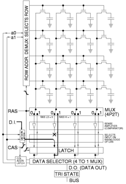
DRAM is usually arranged in a square array of one capacitor and transistor per cell. The illustrations to the right show a simple example with only 4 by 4 cells (modern DRAM can be thousands of cells in length/width).
The long lines connecting each row are known as word lines. Each column is actually composed of two bit lines, each one connected to every other storage cell in the column. (The illustration to the right does not include this important detail.) They are generally known as the + and − bit lines. A sense amplifier is essentially a pair of cross-connected inverters between the bit lines. That is, the first inverter is connected from the + bit line to the − bit line, and the second is connected from the − bit line to the + bit line. This is an example of positive feedback, and the arrangement is only stable with one bit line high and one bit line low.
To read a bit from a column, the following operations take place:
- The sense amplifier is switched off and the bit lines are precharged to exactly matching voltages that are intermediate between high and low logic levels. The bit lines are constructed symmetrically to keep them balanced as precisely as possible.
- The precharge circuit is switched off. Because the bit lines are very long, their capacitance will hold the precharge voltage for a brief time. This is an example of dynamic logic.
- The selected row's word line is driven high. This connects one storage capacitor to one of the two bit lines. Charge is shared between the selected storage cell and the appropriate bit line, slightly altering the voltage on the line. Although every effort is made to keep the capacitance of the storage cells high and the capacitance of the bit lines low, capacitance is proportional to physical size, and the length of the bit lines means that the net effect is a very small perturbation of one bit line's voltage.
- The sense amplifier is switched on. The positive feedback takes over and amplifies the small voltage difference until one bit line is fully low and the other is fully high. At this point, the row is "open" and a column can be selected.
- Read data from the DRAM is taken from the sense amplifiers, selected by the column address. Many reads can be performed while the row is open in this way.
- While reads proceed, current is flowing back up the bit lines from the sense amplifiers to the storage cells. This restores the charge in (refreshes) the storage cell. Due to the length of the bit lines, this takes significant time beyond the end of sense amplification, and overlaps with one or more column reads.
- When done with the current row, the word line is switched off to disconnect the storage capacitors (the row is "closed"), the sense amplifier is switched off, and the bit lines are precharged again.
To write to memory, the row is opened and a given column's sense amplifier is temporarily forced to the desired state, so it drives the bit line which charges the capacitor to the desired value. Due to the positive feedback, the amplifier will then hold it stable even after the forcing is removed. During a write to a particular cell, the entire row is read out, one value changed, and then the entire row is written back in, as illustrated in the figure to the right.
Typically, manufacturers specify that each row should be refreshed every 64 ms or less, according to the JEDEC (Foundation for developing Semiconductor Standards) standard. Refresh logic is commonly used with DRAMs to automate the periodic refresh. This makes the circuit more complicated, but this drawback is usually outweighed by the fact that DRAM is much cheaper and of greater capacity than SRAM. Some systems refresh every row in a tight loop that occurs once every 64 ms. Other systems refresh one row at a time — for example, a system with 213 = 8192 rows would require a refresh rate of one row every 7.8 µs (64 ms / 8192 rows). A few real-time systems refresh a portion of memory at a time based on an external timer that governs the operation of the rest of the system, such as the vertical blanking interval that occurs every 10 to 20 ms in video equipment. All methods require some sort of counter to keep track of which row is the next to be refreshed. Most DRAM chips include that counter; older kinds require external refresh logic to hold that counter. (Under some conditions, most of the data in DRAM can be recovered even if the DRAM has not been refreshed for several minutes. See dynamic random access memory#Security.)
[edit] Memory timing
There are many numbers required to describe the timing of DRAM operation. Here are some examples for two timing grades of asynchronous DRAM, from a data sheet published in 1998:[2]
| "50 ns" | "60 ns" | Description | |
|---|---|---|---|
| tRC | 84 ns | 104 ns | Random read or write cycle time (from one full /RAS cycle to another) |
| tRAC | 50 ns | 60 ns | Access time: /RAS low to valid data out |
| tRCD | 11 ns | 14 ns | /RAS low to /CAS low time |
| tRAS | 50 ns | 60 ns | /RAS pulse width (minimum /RAS low time) |
| tRP | 30 ns | 40 ns | /RAS precharge time (minimum /RAS high time) |
| tPC | 20 ns | 25 ns | Page-mode read or write cycle time (/CAS to /CAS) |
| tAA | 25 ns | 30 ns | Access time: Column address valid to valid data out (includes address setup time before /CAS low) |
| tCAC | 13 ns | 15 ns | Access time: /CAS low to valid data out |
| tCAS | 8 ns | 10 ns | /CAS low pulse width minimum |
Thus, the generally quoted number is the /RAS access time. This is the time to read a random bit from a precharged DRAM array. The time to read additional bits from an open page is much less.
When such a RAM is accessed by clocked logic, the times are generally rounded up to the nearest clock cycle. For example, when accessed by a 100 MHz state machine (i.e. a 10 ns clock), the 50 ns DRAM can perform the first read in 5 clock cycles, and additional reads within the same page every 2 clock cycles. This was generally described as "5-2-2-2" timing, as bursts of 4 reads within a page were common.
When describing synchronous memory, timing is also described by clock cycle counts separated by hyphens, but the numbers have very different meanings! These numbers represent tCL– tRCD– tRP– tRAS in multiples of the DRAM clock cycle time. Note that this is half of the data transfer rate when double data rate signaling is used. JEDEC standard PC3200 timing is 3-4-4-8[3] with a 200 MHz clock, while premium-priced high performance PC3200 DDR DRAM DIMM might be operated at 2-2-2-5 timing.[4]
| PC-3200 (DDR-400) | PC2-6400 (DDR2-800) | PC3-12800 (DDR3-1600) | Description | ||||||||||
|---|---|---|---|---|---|---|---|---|---|---|---|---|---|
| Typical | Fast | Typical | Fast | Typical | Fast | ||||||||
| cycles | time | cycles | time | cycles | time | cycles | time | cycles | time | cycles | time | ||
| tCL | 3 | 15 ns | 2 | 10 ns | 5 | 12.5 ns | 4 | 10 ns | 9 | 11.25 ns | 8 | 10 ns | /CAS low to valid data out (equivalent to tCAC) |
| tRCD | 4 | 20 ns | 2 | 10 ns | 5 | 12.5 ns | 4 | 10 ns | 9 | 11.25 ns | 8 | 10 ns | /RAS low to /CAS low time |
| tRP | 4 | 20 ns | 2 | 10 ns | 5 | 12.5 ns | 4 | 10 ns | 9 | 11.25 ns | 8 | 10 ns | /RAS precharge time (minimum precharge to active time) |
| tRAS | 8 | 40 ns | 5 | 25 ns | 16 | 40 ns | 12 | 30 ns | 27 | 33.75 ns | 24 | 30 ns | Row active time (minimum active to precharge time) |
It is worth noting that the improvement over 11 years is not that large. Minimum random access time has improved from tRAC = 50 ns to tRCD + tCL = 23.5 ns, and even the premium 20 ns variety is only 2.5× better. CAS latency has improved even less, from tCAC = 13 ns to 10 ns. However, the DDR3 memory does achieve 32 times higher bandwidth; due to internal pipelining and wide data paths, it can output two words every 1.25 ns (1600 Mword/s), while the EDO DRAM can output one word per tPC = 20 ns (50 Mword/s).
[edit] Errors and error correction
Electrical or magnetic interference inside a computer system can cause a single bit of DRAM to spontaneously flip to the opposite state. It was initially thought that this was mainly due to alpha particles emitted by contaminants in chip packaging material, but research [5] has shown that the majority of one-off ("soft") errors in DRAM chips occur as a result of background radiation, chiefly neutrons from cosmic ray secondaries which may change the contents of one or more memory cells, or interfere with the circuitry used to read/write them. There is some concern that as DRAM density increases further, and thus the components on DRAM chips get smaller, while at the same time operating voltages continue to fall, DRAM chips will be affected by such radiation more frequently - since lower energy particles will be able to change a memory cell's state. On the other hand, smaller cells make smaller targets, and moves to technologies such as SOI may make individual cells less susceptible and so counteract, or even reverse this trend.
This problem can be mitigated by using DRAM modules that include extra memory bits and memory controllers that exploit these bits. These extra bits are used to record parity or to use an error-correcting code (ECC). Parity allows the detection of a single-bit error (actually, any odd number of wrong bits). The most common error correcting code, Hamming code, allows a single-bit error to be corrected and (in the usual configuration, with an extra parity bit) double-bit errors to be detected.
Error detection and correction in computer systems seems to go in and out of fashion. Seymour Cray famously said "parity is for farmers" when asked why he left this out of the CDC 6600.[2] He included parity in the CDC 7600, and reputedly said "I learned that a lot of farmers buy computers." The original IBM PC and all PCs until the early 1990s used parity checking[3]. Later ones mostly did not. Wider memory buses make parity and especially ECC more affordable. Many current microprocessor memory controllers, including almost all AMD 64-bit offerings, support ECC, but many motherboards and in particular those using low-end chipsets do not.
An ECC-capable memory controller as used in many modern PCs can typically detect and correct errors of a single bit per 64-bit "word" (the unit of bus transfer), and detect (but not correct) errors of two bits per 64-bit word. Where ECC is supported on motherboards suitable for desktop, rather than server, machines ECC can usually be disabled to allow use of non-ECC memory. Some systems also 'scrub' the errors, by writing the corrected version back to memory. The BIOS in some computers, and operating systems such as Linux, allow counting of detected and corrected memory errors, in part to help identify failing memory modules before the problem becomes catastrophic. Most modern PCs do not support ECC at all[contradiction] as can be seen by examining computer and motherboard specifications; those that do are often supplied with memory modules that do not support parity or ECC. It may be that most users opt for non-ECC systems and memory anyway even when ECC is available. The most important reasons for this are:
- the higher cost of ECC memory (each bank is 9 memory chips compared to 8 for non-ECC memory, and more importantly there is more volume for non-ECC. In some cases the price ratio reduces to 9/8, as an example, on 2008/11/30, on Crucial.com, an ECC CL=5 unbuffered 2GB DDR2-667 DIMM costs $30 while the corresponding non-ECC part costs $28, a difference of 1/15, however some ECC modules cost twice as much as their non-ECC equivalents [Crucial CT12872Z40B and CT12864Z40B, Jan 2009]);
- the higher cost of a motherboard that supports ECC functionality in RAM;
- ECC processing is more sensitive to changes in clock speed, making it harder to overclock;[citation needed]
- ECC memory controllers require additional time to perform the error checking and possibly the correction steps, which may lead to an all-around performance hit of around 0.5-2 percent, depending on application[6]; and
- simple ignorance of the issue.
Error detection and correction depends on an expectation of the kinds of errors that occur. Implicitly, we have assumed that the failure of each bit in a word of memory is independent and hence that two simultaneous errors are improbable. This used to be the case when memory chips were one bit wide (typical in the first half of the 1980s). Now many bits are in the same chip. This weakness does not seem to be widely addressed; one exception is Chipkill.
Tests[ecc]give widely varying error rates, but about 10-12upset/bit-hr is typical, roughly one bit error, per month, per gigabyte of memory.
In most computers used for serious scientific or financial computing and as servers, ECC is the rule rather than the exception, as can be seen by examining manufacturers' specifications.
[edit] DRAM packaging
For economic reasons, the large (main) memories found in personal computers, workstations, and non-handheld game-consoles (such as Playstation and Xbox) normally consists of dynamic RAM (DRAM). Other parts of the computer, such as cache memories and data buffers in hard disks, normally use static RAM (SRAM).
[edit] General DRAM packaging formats
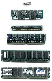
From top to bottom: DIP, SIPP, SIMM 30 pin, SIMM 72 pin, DIMM (168-pin), DDR DIMM (184-pin).
Dynamic random access memory is produced as integrated circuits (ICs) bonded and mounted into plastic packages with metal pins for connection to control signals and buses. Today, these DRAM packages are in turn often assembled into plug-in modules for easier handling. Some standard module types are:
- DRAM chip (Integrated Circuit or IC)
- Dual in-line Package (DIP)
- DRAM (memory) modules
- Single In-line Pin Package (SIPP)
- Single In-line Memory Module (SIMM)
- Dual In-line Memory Module (DIMM)
- Rambus In-line Memory Module (RIMM), technically DIMMs but called RIMMs due to their proprietary slot.
- Small outline DIMM (SO-DIMM), about half the size of regular DIMMs, are mostly used in notebooks, small footprint PCs (such as Mini-ITX motherboards), upgradable office printers and networking hardware like routers. Comes in versions with:
- 72 pins (32-bit)
- 144 pins (64-bit)
- 200 pins (72-bit)
- Small outline RIMM (SO-RIMM). Smaller version of the RIMM, used in laptops. Technically SO-DIMMs but called SO-RIMMs due to their proprietary slot.
- Stacked v. non-stacked RAM modules
- Stacked RAM modules contain two or more RAM chips stacked on top of each other. This allows large modules (like 512mb or 1Gig SO-DIMM) to be manufactured using cheaper low density wafers. Stacked chip modules draw more power.
[edit] Common DRAM modules
Common DRAM packages as illustrated to the right, from top to bottom:
- DIP 16-pin (DRAM chip, usually pre-FPRAM)
- SIPP (usually FPRAM)
- SIMM 30-pin (usually FPRAM)
- SIMM 72-pin (often EDO RAM but FPM is not uncommon)
- DIMM 168-pin (SDRAM)
- DIMM 184-pin (DDR SDRAM)
- RIMM 184-pin
- DIMM 240-pin (DDR2 SDRAM/DDR3 SDRAM)
[edit] Variations
While the fundamental DRAM cell and array has maintained the same basic structure (and performance) for many years, there have been many different interfaces for speaking with DRAM chips. When one speaks about "DRAM types", one is generally referring to the interface that is used.
[edit] Asynchronous DRAM
This is the basic form, from which all others are derived. An asynchronous DRAM chip has power connections, some number of address inputs (typically 12), and a few (typically 1 or 4) bidirectional data lines. There are four active low control signals:
- /RAS, the Row Address Strobe. The address inputs are captured on the falling edge of /RAS, and select a row to open. The row is held open as long as /RAS is low.
- /CAS, the Column Address Strobe. The address inputs are captured on the falling edge of /CAS, and select a column from the currently open row to read or write.
- /WE, Write Enable. This signal determines whether a given falling edge of /CAS is a read (if high) or write (if low). If low, the data inputs are also captured on the falling edge of /CAS.
- /OE, Output Enable. This is an additional signal that controls output to the data I/O pins. The data pins are driven by the DRAM chip if /RAS and /CAS are low, /WE is high, and /OE is low. In many applications, /OE can be permanently connected low (output always enabled), but it can be useful when connecting multiple memory chips in parallel.
This interface provides direct control of internal timing. When /RAS is driven low, a /CAS cycle must not be attempted until the sense amplifiers have sensed the memory state, and /RAS must not be returned high until the storage cells have been refreshed. When /RAS is driven high, it must be held high long enough for precharging to complete.
[edit] Video DRAM (VRAM)
VRAM is a dual-ported variant of DRAM which was once commonly used to store the frame-buffer in some graphics adaptors.
It was invented by F. Dill and R. Matick at IBM Research in 1980, with a patent issued in 1985 (US Patent 4,541,075). The first commercial use of VRAM was in the high resolution graphics adapter introduced in 1986 by IBM with the PC/RT system.
VRAM has two sets of data output pins, and thus two ports that can be used simultaneously. The first port, the DRAM port, is accessed by the host computer in a manner very similar to traditional DRAM. The second port, the video port, is typically read-only and is dedicated to providing a high bandwidth data channel for the graphics chipset.[7]
Typical DRAM arrays normally access a full row of bits (i.e. a word line) at up to 1024 bits at one time, but only use one or a few of these for actual data, the remainder being discarded. Since DRAM cells are destructively read, each bit accessed must be sensed, and re-written. Thus, typically, 1024 sense amplifiers are typically used. VRAM operates by not discarding the excess bits which must be accessed, but making full use of them in a simple way. If each horizontal scan line of a display is mapped to a full word, then upon reading one word and latching all 1024 bits into a separate row buffer, these bits can subsequently be serially streamed to the display circuitry. This will leave access to the DRAM array free to be accessed (read or write) for many cycles, until the row buffer is almost depleted. A complete DRAM read cycle is only required to fill the row buffer, leaving most DRAM cycles available for normal accesses.
Such operation is described in the paper "All points addressable raster display memory" by R. Matick, D. Ling, S. Gupta, and F. Dill, IBM Journal of R&D, Vol 28, No. 4, July 1984, pp379-393. To use the video port, the controller first uses the DRAM port to select the row of the memory array that is to be displayed. The VRAM then copies that entire row to an internal row-buffer which is a shift-register. The controller can then continue to use the DRAM port for drawing objects on the display. Meanwhile, the controller feeds a clock called the shift clock (SCLK) to the VRAM's video port. Each SCLK pulse causes the VRAM to deliver the next datum, in strict address order, from the shift-register to the video port. For simplicity, the graphics adapter is usually designed so that the contents of a row, and therefore the contents of the shift-register, corresponds to a complete horizontal line on the display.
In the late 1990s, standard DRAM technologies (e.g. SDRAM) became cheap, dense, and high performance enough to completely displace VRAM, even though it was only single-ported and some memory bits were wasted.
[edit] Fast Page Mode (FPM) DRAM or FPRAM

Fast page mode DRAM is also called FPM DRAM, Page mode DRAM, Fast page mode memory, or Page mode memory.
In page mode, a row of the DRAM can be kept "open" by holding /RAS low while performing multiple reads or writes with separate pulses of /CAS. so that successive reads or writes within the row do not suffer the delay of precharge and accessing the row. This increases the performance of the system when reading or writing bursts of data.
Static column is a variant of page mode in which the column address does not need to be strobed in, but rather, the address inputs may be changed with /CAS held low, and the data output will be updated accordingly a few nanoseconds later.
Nibble mode is another variant in which four sequential locations within the row can be accessed with four consecutive pulses of /CAS. The difference from normal page mode is that the address inputs are not used for the second through fourth /CAS edges; they are generated internally starting with the address supplied for the first /CAS edge.
[edit] CAS before RAS refresh
Classic asynchronous DRAM is refreshed by opening each row in turn. This can be done by supplying a row address and pulsing /RAS low; it is not necessary to perform any /CAS cycles. An external counter is needed to iterate over the row addresses in turn.
For convenience, the counter was quickly incorporated into RAM chips themselves. If the /CAS line is driven low before /RAS (normally an illegal operation), then the DRAM ignores the address inputs and uses an internal counter to select the row to open. This is known as /CAS-before-/RAS (CBR) refresh.
This became the standard form of refresh for asynchronous DRAM, and is the only form generally used with SDRAM.
[edit] Extended Data Out (EDO) DRAM

EDO DRAM is similar to Fast Page Mode DRAM with the additional feature that a new access cycle can be started while keeping the data output of the previous cycle active. This allows a certain amount of overlap in operation (pipelining), allowing somewhat improved performance. It was 5% faster than Fast Page Mode DRAM, which it began to replace in 1993.
To be precise, EDO DRAM begins data output on the falling edge of /CAS, but does not stop the output when /CAS rises again. It holds the output valid (thus extending the data output time) until either /RAS is deasserted, or a new /CAS falling edge selects a different column address.
Single-cycle EDO has the ability to carry out a complete memory transaction in one clock cycle. Otherwise, each sequential RAM access within the same page takes two clock cycles instead of three, once the page has been selected. EDO's performance and capabilities allowed it to somewhat replace the then-slow L2 caches of PCs. It created an opportunity to reduce the immense performance loss associated with a lack of L2 cache, while making systems cheaper to build. This was also good for notebooks due to difficulties with their limited form factor, and battery life limitations. An EDO system with L2 cache was tangibly faster than the older FPM/L2 combination.
Single-cycle EDO DRAM became very popular on video cards towards the end of the 1990s. It was very low cost, yet nearly as efficient for performance as the far more costly VRAM.
EDO was sometimes referred to as Hyper Page Mode.
Much equipment taking 72-pin SIMMs could use either FPM or EDO. Problems were possible, particularly when mixing FPM and EDO. Early Hewlett-Packard printers had FPM RAM built in; some, but not all, models worked if additional EDO SIMMs were added[8].
[edit] Burst EDO (BEDO) DRAM
An evolution of the former, Burst EDO DRAM, could process four memory addresses in one burst, for a maximum of 5-1-1-1, saving an additional three clocks over optimally designed EDO memory. It was done by adding an address counter on the chip to keep track of the next address. BEDO also added a pipelined stage allowing page-access cycle to be divided into two components. During a memory-read operation, the first component accessed the data from the memory array to the output stage (second latch). The second component drove the data bus from this latch at the appropriate logic level. Since the data is already in the output buffer, quicker access time is achieved (up to 50% for large blocks of data) than with traditional EDO.
Although BEDO DRAM showed additional optimization over EDO, by the time it was available the market had made a significant investment towards synchronous DRAM, or SDRAM [4]. Even though BEDO RAM was superior to SDRAM in some ways, the latter technology gained significant traction and quickly displaced BEDO.
[edit] Multibank DRAM (MDRAM)
Multibank RAM applies the interleaving technique for main memory to second level cache memory to provide a cheaper and faster alternative to SRAM. The chip splits its memory capacity into small blocks of 256 kB and allows operations to two different banks in a single clock cycle.
This memory was primarily used in graphic cards with Tseng Labs ET6x00 chipsets, and was made by MoSys. Boards based upon this chipset often used the unusual RAM size configuration of 2.25 MB, owing to MDRAM's ability to be implemented in various sizes more easily. This size of 2.25 MB allowed 24-bit color at a resolution of 1024×768, a very popular display setting in the card's time.
[edit] Synchronous Graphics RAM (SGRAM)
SGRAM is a specialized form of SDRAM for graphics adaptors. It adds functions such as bit masking (writing to a specified bit plane without affecting the others) and block write (filling a block of memory with a single colour). Unlike VRAM and WRAM, SGRAM is single-ported. However, it can open two memory pages at once, which simulates the dual-port nature of other video RAM technologies.
[edit] Synchronous Dynamic RAM (SDRAM)
Single Data Rate (SDR) SDRAM is a synchronous form of DRAM.
[edit] Direct Rambus DRAM (DRDRAM)
Direct RAMBUS DRAM (DRDRAM).....
[edit] Double Data Rate (DDR) SDRAM
Double data rate (DDR) SDRAM was a later development of SDRAM, used in PC memory beginning in 2000. DDR2 SDRAM was originally seen as a minor enhancement (based upon the industry standard single-core CPU) on DDR SDRAM that mainly afforded higher clock rates and somewhat deeper pipelining. However, with the introduction and rapid acceptance of the multi-core CPU in 2006, it is generally expected in the industry that DDR2 will revolutionize the existing physical DDR-SDRAM standard. Further, with the development and introduction of DDR3 SDRAM in 2007, it is anticipated DDR3 will rapidly replace the more limited DDR and newer DDR2.The reason for the use of DDR DRAM is that it has a high data rate multiple of two thaan SDRAM.
[edit] Pseudostatic RAM (PSRAM)
PSRAM or PSDRAM is dynamic RAM with built-in refresh and address-control circuitry to make it behave similarly to static RAM (SRAM). It combines the high density of DRAM with the ease of use of true SRAM. PSRAM (made by Numonyx) is used in the Apple iPhone and other embedded systems[9]
Some DRAM components have a "self-refresh mode". While this involves much of the same logic that is needed for pseudo-static operation, this mode is often equivalent to a standby mode. It is provided primarily to allow a system to suspend operation of its DRAM controller to save power without losing data stored in DRAM, not to allow operation without a separate DRAM controller as is the case with PSRAM.
An embedded variant of pseudostatic RAM is sold by MoSys under the name 1T-SRAM. It is technically DRAM, but behaves much like SRAM. It is used in Nintendo Gamecube and Wii consoles.
[edit] 1T DRAM
Unlike all of the other variants described here, 1T DRAM is actually a different way of constructing the basic DRAM bit cell. 1T DRAM is a "capacitorless" bit cell design that stores data in the parasitic body capacitor that is an inherent part of Silicon on Insulator transistors. Considered a nuisance in logic design, this floating body effect can be used for data storage. Although refresh is still required, reads are non-destructive; the stored charge causes a detectable shift in the threshold voltage of the transistor.Sallese, Jean-Michel (2002-06-20). "Principles of the 1T Dynamic Access Memory Concept on SOI". MOS Modeling and Parameter Extraction Group Meeting. Retrieved on 2007-10-07.
1T DRAM is commercialized under the name Z-RAM.
Note that classic one-transistor/one-capacitor (1T/1C) DRAM cell is also sometimes referred to as "1T DRAM".
[edit] RLDRAM
Reduced Latency DRAM is a high performance double data rate (DDR) SDRAM that combines fast, random access with high bandwidth. RLDRAM is mainly designed for networking and caching applications.
[edit] Security
Although dynamic memory is only guaranteed to retain its contents when supplied with power and refreshed every 64 ms, the memory cell capacitors will often retain their values for significantly longer, particularly at low temperatures.[10]
Under some conditions, most of the data in DRAM can be recovered even if the DRAM has not been refreshed for several minutes.[11]
This property can be used to recover "secure" data kept in memory by quickly rebooting the computer and dumping the contents of the RAM or by cooling the chips and transferring them to a different computer. Such an attack was demonstrated to circumvent popular disk encryption systems, like the open source TrueCrypt, Microsoft's BitLocker Drive Encryption, as well as Apple's FileVault.[10]
[edit] DRAM Memory Timings Acronyms
Some of the timing jargons appear a little bit cryptic in the BIOS settings. Here is a list of acronyms:
- CL: CAS Latency
- CR: Command Rate
- tPTP: Precharge To Precharge Delay
- tRAS: RAS Active Time
- tRCD: RAS To CAS Delay
- tREF: Refresh Period
- tRFC: Row Refresh Cycle Time
- tRP: RAS Precharge
- tRRD: RAS To RAS Delay
- tRTP: Read To Precharge Delay
- tRTR: Read To Read Delay
- tRTW: Read To Write Delay
- tWR: Write Recovery Time
- tWTP: Write To Precharge Delay
- tWTR: Write To Read Delay
- tWTW: Write To Write Delay
[edit] See also
- DRAM price fixing
- DIMM
- Flash memory
- Regenerative capacitor memory
- Static random access memory
- List of device bandwidths
[edit] References
- ^ Toshiba "Toscal" BC-1411 Desktop Calculator
- ^ Micron 4 Meg x 4 EDO DRAM data sheet
- ^ cmx1024-3200.ai
- ^ http://www.corsairmemory.com/corsair/products/specs/twinx1024-3200xl.pdf
- ^ [1] Single Event Upset at Ground Level, Eugene Normand, Member, IEEE, Boeing Defense & Space Group, Seattle, WA 98124-2499
- ^ Discussion of ECC on pcguide
- ^ SM55161A 262144×16 bit VRAM data sheet, Austin Semiconductor, http://www.austinsemiconductor.com/datasheet/Austin-Semiconductor-Datasheet-SM55161A.PDF, retrieved on 2009-03-02
- ^ Page on memory upgrades for HP printers
- ^ EE Times teardown of iPhone 3G
- ^ a b "Center for Information Technology Policy » Lest We Remember: Cold Boot Attacks on Encryption Keys". http://citp.princeton.edu/memory/. 080222 citp.princeton.edu
- ^ Scheick, Leif Z.; Guertin, Steven M.; Swift, Gary M. (December 2000), "Analysis of radiation effects on individual DRAM cells" (PDF), IEEE Trans. on Nuclear Science 47 (6): 2534–2538, doi:, ISSN 0018-9499, http://parts.jpl.nasa.gov/docs/DRAM_Indiv-00.pdf, retrieved on 2008-11-03
[edit] External links
- DRAM density and speed trends has some interesting historical trend charts of DRAM density and speed from 1980.
- Back to Basics - Memory, part 3
- Benefits of Chipkill-Correct ECC for PC Server Main Memory - A 1997 discussion of SDRAM reliability - some interesting information on "soft errors" from cosmic rays, especially with respect to Error-correcting code schemes
- a Tezzaron Semiconductor Soft Error White Paper 1994 literature review of memory error rate measurements.
- Soft errors' impact on system reliability - Ritesh Mastipuram and Edwin C Wee, Cypress Semiconductor, 2004
- Scaling and Technology Issues for Soft Error Rates - A Johnston - 4th Annual Research Conference on Reliability Stanford University, October 2000
- Challenges and future directions for the scaling of dynamic random-access memory (DRAM) - J. A. Mandelman, R. H. Dennard, G. B. Bronner, J. K. DeBrosse, R. Divakaruni, Y. Li, and C. J. Radens, IBM 2002
- Ars Technica: RAM Guide
- Versatile DRAM interface for the 6502 CPU
- David Tawei Wang (2005). Modern DRAM Memory Systems: Performance Analysis and a High Performance, Power-Constrained DRAM-Scheduling Algorithm. PhD thesis, University of Maryland, College Park. http://www.ece.umd.edu/~blj/papers/thesis-PhD-wang--DRAM.pdf. Retrieved on 2007-03-10. A detailed description of current DRAM technology.
- The Toshiba "Toscal" BC-1411 Desktop Calculator - An early electronic calculator that uses a form of dynamic RAM built from discrete components.
- Mitsubishi's 3D-RAM And Cache DRAM incorporate high performance, on-board SRAM cache
- Multi-port Cache DRAM - MP-RAM
- DRAM timings explained
- How to install DRAM installation guide for desktop and laptop computers.
- DRAM Technology Education
|
||||||||||||||

