Northbridge (computing)
From Wikipedia, the free encyclopedia
| This article needs additional citations for verification. Please help improve this article by adding reliable references (ideally, using inline citations). Unsourced material may be challenged and removed. (January 2008) |
The northbridge, also known as a memory controller hub (MCH) or an integrated memory controller (IMC) in Intel systems (AMD, VIA, SiS and others usually use 'northbridge'), is one of the two chips in the core logic chipset on a PC motherboard, the other being the southbridge. Separating the chipset into the northbridge and southbridge is common, although there are rare instances where these two chips have been combined onto one die when design complexity and fabrication processes permit it.
Contents |
[edit] Overview
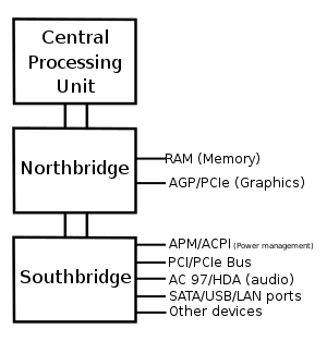
The northbridge typically handles communications among the CPU, RAM, AGP or PCI Express, and the southbridge.[1][2] Some northbridges also contain integrated video controllers, also known as a Graphics and Memory Controller Hub (GMCH) in Intel systems. Because different processors and RAM require different signalling, a northbridge will typically work with only one or two classes of CPUs and generally only one type of RAM. There are a few chipsets that support two types of RAM (generally these are available when there is a shift to a new standard). For example, the northbridge from the NVIDIA nForce2 chipset will only work with Socket A processors combined with DDR SDRAM, the Intel i875 chipset will only work with systems using Pentium 4 processors or Celeron processors that have a clock speed greater than 1.3 GHz and utilize DDR SDRAM, and the Intel i915g chipset only works with the Intel Pentium 4 and the Celeron, but it can use DDR or DDR2 memory.
[edit] Etymology
The name is derived from drawing the architecture in the fashion of a map. The CPU would be at the top of the map comparable to due north on most general purpose geographical maps. The CPU would be connected to the chipset via a fast bridge (the northbridge) located north of other system devices as drawn. The northbridge would then be connected to the rest of the chipset via a slow bridge (the southbridge) located south of other system devices as drawn.

[edit] Importance
The northbridge on a particular system's motherboard is the most prominent factor in dictating the number, speed, and type of CPU(s) and the amount, speed, and type of RAM that can be used. Other factors such as voltage regulation and available number of connectors also play a role. Virtually all consumer-level chipsets support only one processor series, with the maximum amount of RAM varying by processor type and motherboard design. Pentium-era machines often had a limitation of 128 MB, while most Pentium 4 machines have a limit of 4 GB. Since the Pentium Pro, the Intel architecture can accommodate physical addresses larger than 32 bits, typically 36 bits, which gives up to 64 GB of addressing (see PAE), though motherboards that can support that much RAM are rare because of other factors (operating system limitations and expense of RAM).
A northbridge typically will only work with one or two different southbridges. In this respect, it affects some of the other features that a given system can have by limiting which technologies are available on its southbridge partner.
The northbridge hosts its own memory lookup table (I/O memory management unit), a mapping of the addresses and layout in main memory. The northbridge handles data transactions for the front side bus (FSB), the memory bus and the AGP port.
The northbridge will have a different model number, even though they are often paired with the same southbridge to come under the collective name of the chipset.
The Intel Hub Architecture (IHA) has replaced the northbridge/southbridge chipset. The IHA chipset also has two parts: the Graphics and AGP Memory Controller Hub (GMCH) and the I/O Controller Hub (ICH). The IHA architecture is used in Intel's 800 series chipsets, which is the first x86 chipset architecture to move away from the northbridge/southbridge design.
[edit] Recent developments
The memory controller, which handles communication between the CPU and RAM, has been moved onto the processor die in AMD64 processors. Intel has integrated the memory controller onto the processor die with their Nehalem microarchitecture-based processors.
An example of this change is NVIDIA's nForce3 chipset for AMD64 systems that is a single chip. It combines all of the features of a normal southbridge with an AGP port and connects directly to the CPU. On nForce4 boards they consider this to be an MCP (Media Communications Processor).
[edit] Northbridge and overclocking
The northbridge plays an important part in how far a computer can be overclocked, as its frequency is used as a baseline for the CPU to establish its own operating frequency. In today's machines, this chip is becoming increasingly hotter as computers become faster and thus also requires an increased level of cooling.
[edit] See also
[edit] References
- ^ InformIT: Motherboards & Core-Logic Chipsets: The Deep Stuff > What the North Bridge and South Bridge Do
- ^ George Jones - Maximum PC 2005 Buyer's Guide - Prentice Hall PTR - ISBN 0768663121


