Semiconductor
From Wikipedia, the free encyclopedia
|
|
This article may require cleanup to meet Wikipedia's quality standards. Please improve this article if you can. (June 2008) |
|
|
This article is missing citations or needs footnotes. Please help add inline citations to guard against copyright violations and factual inaccuracies. (March 2008) |
A semiconductor is a material that has electrical conductivity between those of a conductor and an insulator. The conductivity of a semiconductor material can be varied under an external electrical field. Devices made from semiconductor materials are the foundation of modern electronics, including radio, computers, telephones, and many other devices. Semiconductor devices include the transistor, many kinds of diodes including the light-emitting diode, the silicon controlled rectifier, and digital and analog integrated circuits. Solar photovoltaic panels are large semiconductor devices that directly convert light energy into electrical energy.
In a metallic conductor, current is carried by the flow of electrons. In semiconductors, current can be carried either by the flow of electrons or by the flow of positively-charged "holes" in the electron structure of the material.
Silicon is used to create most semiconductors commercially. Dozens of other materials are used, including germanium, gallium arsenide, and silicon carbide. A pure semiconductor is often called an “intrinsic” semiconductor. The conductivity, or ability to conduct, of semiconductor material can be drastically changed by adding other elements, called “impurities” to the melted intrinsic material and then allowing the melt to solidify into a new and different crystal. This process is called "doping".[1]
Contents |
[edit] Explaining semiconductor energy bands
There are three popular ways to describe the electronic structure of a crystal.
- Band structure
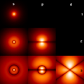 In a single H-atom an electron resides in well known orbits. Note that the orbits are called s,p,d in order of increasing circular current. |
 Putting two atoms together leads to delocalized orbits across two atoms, yielding a covalent bond. Due to the Pauli exclusion principle, every state can contain only one electron. |
 This can be continued with more atoms. Note: This picture shows a metal, not an actual semiconductor. |
 Continuing to add creates a crystal, which may then be cut into a tape and fused together at the ends to allow circular currents. |
 For this regular solid the band structure can be calculated or measured. |
 Integrating over the k axis gives the bands of a semiconductor showing a full valence band and an empty conduction band. Generally stopping at the vacuum level is undesirable, because some people want to calculate: photoemission, inverse photoemission |
 After the band structure is determined states can be combined to generate wave packets. As this is analogous to wave packages in free space, the results are similar. |
An alternative description, which does not really appreciate the strong Coulomb interaction, shoots free electrons into the crystal and looks at the scattering. |
A third alternative description uses strongly localized unpaired electrons in chemical bonds, which looks almost like a Mott insulator. |
[edit] Energy bands and electrical conduction
Like in other solids, the electrons in semiconductors can have energies only within certain bands (ie. ranges of levels of energy) between the energy of the ground state, corresponding to electrons tightly bound to the atomic nuclei of the material, and the free electron energy, which is the energy required for an electron to escape entirely from the material. The energy bands each correspond to a large number of discrete quantum states of the electrons, and most of the states with low energy (closer to the nucleus) are full, up to a particular band called the valence band. Semiconductors and insulators are distinguished from metals because the valence band in the semiconductor materials is very nearly full under usual operating conditions, thus causing more electrons to be available in the conduction band.
The ease with which electrons in a semiconductor can be excited from the valence band to the conduction band depends on the band gap between the bands, and it is the size of this energy bandgap that serves as an arbitrary dividing line (roughly 4 eV) between semiconductors and insulators.
In the picture of covalent bonds, an electron moves by hopping to a neighboring bond. Because of the Pauli exclusion principle it has to be lifted into the higher anti-bonding state of that bond. In the picture of delocalized states, for example in one dimension that is in a wire, for every energy there is a state with electrons flowing in one direction and one state for the electrons flowing in the other. For a net current to flow some more states for one direction than for the other direction have to be occupied and for this energy is needed. For a metal this can be a very small energy in the semiconductor the next higher states lie above the band gap. Often this is stated as: full bands do not contribute to the electrical conductivity. However, as the temperature of a semiconductor rises above absolute zero, there is more energy in the semiconductor to spend on lattice vibration and — more importantly for us — on lifting some electrons into an energy states of the conduction band, which is the band immediately above the valence band. The current-carrying electrons in the conduction band are known as "free electrons", although they are often simply called "electrons" if context allows this usage to be clear.
Electrons excited to the conduction band also leave behind electron holes, or unoccupied states in the valence band. Both the conduction band electrons and the valence band holes contribute to electrical conductivity. The holes themselves don't actually move, but a neighboring electron can move to fill the hole, leaving a hole at the place it has just come from, and in this way the holes appear to move, and the holes behave as if they were actual positively charged particles.
One covalent bond between neighboring atoms in the solid is ten times stronger than the binding of the single electron to the atom, so freeing the electron does not imply destruction of the crystal structure.
[edit] Holes: electron absence as a charge carrier
The notion of holes, which was introduced for semiconductors, can also be applied to metals, where the Fermi level lies within the conduction band. With most metals the Hall effect reveals electrons to be the charge carriers, but some metals have a mostly filled conduction band, and the Hall effect reveals positive charge carriers, which are not the ion-cores, but holes. Contrast this to some conductors like solutions of salts, or plasma. In the case of a metal, only a small amount of energy is needed for the electrons to find other unoccupied states to move into, and hence for current to flow. Sometimes even in this case it may be said that a hole was left behind, to explain why the electron does not fall back to lower energies: It cannot find a hole. In the end in both materials electron-phonon scattering and defects are the dominant causes for resistance.

The energy distribution of the electrons determines which of the states are filled and which are empty. This distribution is described by Fermi-Dirac statistics. The distribution is characterized by the temperature of the electrons, and the Fermi energy or Fermi level. Under absolute zero conditions the Fermi energy can be thought of as the energy up to which available electron states are occupied. At higher temperatures, the Fermi energy is the energy at which the probability of a state being occupied has fallen to 0.5.
The dependence of the electron energy distribution on temperature also explains why the conductivity of a semiconductor has a strong temperature dependency, as a semiconductor operating at lower temperatures will have fewer available free electrons and holes able to do the work.
[edit] Energy–momentum dispersion
In the preceding description an important fact is ignored for the sake of simplicity: the dispersion of the energy. The reason that the energies of the states are broadened into a band is that the energy depends on the value of the wave vector, or k-vector, of the electron. The k-vector, in quantum mechanics, is the representation of the momentum of a particle.
The dispersion relationship determines the effective mass, m * , of electrons or holes in the semiconductor, according to the formula:
![m^{*} = \hbar^2 \cdot \left[ {{d^2 E(k)} \over {d k^2}} \right]^{-1}](http://upload.wikimedia.org/math/b/1/a/b1a58d209be0a622c0d09a2e24ce01fa.png)
The effective mass is important as it affects many of the electrical properties of the semiconductor, such as the electron or hole mobility, which in turn influences the diffusivity of the charge carriers and the electrical conductivity of the semiconductor.
Typically the effective mass of electrons and holes are different. This affects the relative performance of p-channel and n-channel IGFETs, for example (Muller & Kamins 1986:427).
The top of the valence band and the bottom of the conduction band might not occur at that same value of k. Materials with this situation, such as silicon and germanium, are known as indirect bandgap materials. Materials in which the band extrema are aligned in k, for example gallium arsenide, are called direct bandgap semiconductors. Direct gap semiconductors are particularly important in optoelectronics because they are much more efficient as light emitters than indirect gap materials.
[edit] Carrier generation and recombination
When ionizing radiation strikes a semiconductor, it may excite an electron out of its energy level and consequently leave a hole. This process is known as electron–hole pair generation. Electron-hole pairs are constantly generated from thermal energy as well, in the absence of any external energy source.
Electron-hole pairs are also apt to recombine. Conservation of energy demands that these recombination events, in which an electron loses an amount of energy larger than the band gap, be accompanied by the emission of thermal energy (in the form of phonons) or radiation (in the form of photons).
In some states, the generation and recombination of electron–hole pairs are in equipoise. The number of electron-hole pairs in the steady state at a given temperature is determined by quantum statistical mechanics. The precise quantum mechanical mechanisms of generation and recombination are governed by conservation of energy and conservation of momentum.
As the probability that electrons and holes meet together is proportional to the product of their amounts, the product is in steady state nearly constant at a given temperature, providing that there is no significant electric field (which might "flush" carriers of both types, or move them from neighbour regions containing more of them to meet together) or externally driven pair generation. The product is a function of the temperature, as the probability of getting enough thermal energy to produce a pair increases with temperature, being approximately 1×exp(−EG / kT), where k is Boltzmann's constant, T is absolute temperature and EG is band gap.
The probability of meeting is increased by carrier traps – impurities or dislocations which can trap an electron or hole and hold it until a pair is completed. Such carrier traps are sometimes purposely added to reduce the time needed to reach the steady state.
[edit] Doping
The property of semiconductors that makes them most useful for constructing electronic devices is that their conductivity may easily be modified by introducing impurities into their crystal lattice. The process of adding controlled impurities to a semiconductor is known as doping. The amount of impurity, or dopant, added to an intrinsic (pure) semiconductor varies its level of conductivity. Doped semiconductors are often referred to as extrinsic. By adding impurity to pure semiconductors, the electrical conductivity may be varied not only by the number of impurity atoms but also, by the type of impurity atom and the changes may be thousand folds and million folds. For example - 1 cm3 of a metal or semiconductor specimen has a number of atoms of the order of 1022. Since every atom in metal donates at least one free electron for conduction in metal, 1 cm3 of metal contains number of free electrons in the order of 1022. At the temperature close to 20 °C , 1 cm3 of pure germanium contains about 4.2 × 10²² atoms and 2.5 × 10¹³ free electrons and 2.5 × 10¹³ holes (empty spaces in crystal lattice having positive charge) The addition of 0.001% of arsenic (impurity) donates extra 1017 free electrons in the same volume and the electrical conductivity increases about 10,000 times. "
[edit] Dopants
The materials chosen as suitable dopants depend on the atomic properties of both the dopant and the material to be doped. In general, dopants that produce the desired controlled changes are classified as either electron acceptors or donors. A donor atom that activates (that is, becomes incorporated into the crystal lattice) donates weakly-bound valence electrons to the material, creating excess negative charge carriers. These weakly-bound electrons can move about in the crystal lattice relatively freely and can facilitate conduction in the presence of an electric field. (The donor atoms introduce some states under, but very close to the conduction band edge. Electrons at these states can be easily excited to conduction band, becoming free electrons, at room temperature.) Conversely, an activated acceptor produces a hole. Semiconductors doped with donor impurities are called n-type, while those doped with acceptor impurities are known as p-type. The n and p type designations indicate which charge carrier acts as the material's majority carrier. The opposite carrier is called the minority carrier, which exists due to thermal excitation at a much lower concentration compared to the majority carrier.
For example, the pure semiconductor silicon has four valence electrons. In silicon, the most common dopants are IUPAC group 13 (commonly known as group III) and group 15 (commonly known as group V) elements. Group 13 elements all contain three valence electrons, causing them to function as acceptors when used to dope silicon. Group 15 elements have five valence electrons, which allows them to act as a donor. Therefore, a silicon crystal doped with boron creates a p-type semiconductor whereas one doped with phosphorus results in an n-type material.
[edit] Carrier concentration
The concentration of dopant introduced to an intrinsic semiconductor determines its concentration and indirectly affects many of its electrical properties. The most important factor that doping directly affects is the material's carrier concentration. In an intrinsic semiconductor under thermal equilibrium, the concentration of electrons and holes is equivalent. That is,
- n = p = ni
If we have a non-intrinsic semiconductor in thermal equilibrium the relation becomes:
- n0 * p0 = (ni)2
Where n0 is the concentration of conducting electrons, p0 is the electron hole concentration, and ni is the material's intrinsic carrier concentration. Intrinsic carrier concentration varies between materials and is dependent on temperature. Silicon's ni, for example, is roughly 1.0×1010 cm-3 at 300 kelvin (room temperature).
In general, an increase in doping concentration affords an increase in conductivity due to the higher concentration of carriers available for conduction. Degenerately (very highly) doped semiconductors have conductivity levels comparable to metals and are often used in modern integrated circuits as a replacement for metal. Often superscript plus and minus symbols are used to denote relative doping concentration in semiconductors. For example, n + denotes an n-type semiconductor with a high, often degenerate, doping concentration. Similarly, p − would indicate a very lightly doped p-type material. It is useful to note that even degenerate levels of doping imply low concentrations of impurities with respect to the base semiconductor. In crystalline intrinsic silicon, there are approximately 5×10²² atoms/cm³. Doping concentration for silicon semiconductors may range anywhere from 1013 cm-3 to 1018 cm-3. Doping concentration above about 1018 cm-3 is considered degenerate at room temperature. Degenerately doped silicon contains a proportion of impurity to silicon in the order of parts per thousand. This proportion may be reduced to parts per billion in very lightly doped silicon. Typical concentration values fall somewhere in this range and are tailored to produce the desired properties in the device that the semiconductor is intended for.
[edit] Effect on band structure

Doping a semiconductor crystal introduces allowed energy states within the band gap but very close to the energy band that corresponds to the dopant type. In other words, donor impurities create states near the conduction band while acceptors create states near the valence band. The gap between these energy states and the nearest energy band is usually referred to as dopant-site bonding energy or EB and is relatively small. For example, the EB for boron in silicon bulk is 0.045 eV, compared with silicon's band gap of about 1.12 eV. Because EB is so small, it takes little energy to ionize the dopant atoms and create free carriers in the conduction or valence bands. Usually the thermal energy available at room temperature is sufficient to ionize most of the dopant.
Dopants also have the important effect of shifting the material's Fermi level towards the energy band that corresponds with the dopant with the greatest concentration. Since the Fermi level must remain constant in a system in thermodynamic equilibrium, stacking layers of materials with different properties leads to many useful electrical properties. For example, the p-n junction's properties are due to the energy band bending that happens as a result of lining up the Fermi levels in contacting regions of p-type and n-type material.
This effect is shown in a band diagram. The band diagram typically indicates the variation in the valence band and conduction band edges versus some spatial dimension, often denoted x. The Fermi energy is also usually indicated in the diagram. Sometimes the intrinsic Fermi energy, Ei, which is the Fermi level in the absence of doping, is shown. These diagrams are useful in explaining the operation of many kinds of semiconductor devices.
[edit] Preparation of semiconductor materials
Semiconductors with predictable, reliable electronic properties are necessary for mass production. The level of chemical purity needed is extremely high because the presence of impurities even in very small proportions can have large effects on the properties of the material. A high degree of crystalline perfection is also required, since faults in crystal structure (such as dislocations, twins, and stacking faults) interfere with the semiconducting properties of the material. Crystalline faults are a major cause of defective semiconductor devices. The larger the crystal, the more difficult it is to achieve the necessary perfection. Current mass production processes use crystal ingots between four and twelve inches (300 mm) in diameter which are grown as cylinders and sliced into wafers.
Because of the required level of chemical purity and the perfection of the crystal structure which are needed to make semiconductor devices, special methods have been developed to produce the initial semiconductor material. A technique for achieving high purity includes growing the crystal using the Czochralski process. An additional step that can be used to further increase purity is known as zone refining. In zone refining, part of a solid crystal is melted. The impurities tend to concentrate in the melted region, while the desired material recrystalizes leaving the solid material more pure and with fewer crystalline faults.
In manufacturing semiconductor devices involving heterojunctions between different semiconductor materials, the lattice constant, which is the length of the repeating element of the crystal structure, is important for determining the compatibility of materials.
[edit] See also
[edit] References
- ^ International Union of Pure and Applied Chemistry. "semiconductor". Compendium of Chemical Terminology Internet edition.
- Notes
- A. A. Balandin and K. L. Wang (2006), Handbook of Semiconductor Nanostructures and Nanodevices (5-Volume Set), American Scientific Publishers. ISBN 1-58883-073-X
- Muller, Richard S.; Theodore I. Kamins (1986). Device Electronics for Integrated Circuits (2d ed.). New York: Wiley. ISBN 0-471-88758-7.
- Sze, Simon M. (1981). Physics of Semiconductor Devices (2nd ed.). John Wiley and Sons (WIE). ISBN 0-471-05661-8.
- Turley, Jim (2002). The Essential Guide to Semiconductors. Prentice Hall PTR. ISBN 0-13-046404-X.
- Yu, Peter Y.; Cardona, Manuel (2004). Fundamentals of Semiconductors : Physics and Materials Properties. Springer. ISBN 3-540-41323-5.
- Ben G. Steetman and Sanjay Kumar Banerjee (2006), Solid State Electronic Devices, Pearson Education Inc. ISBN 0-13-149726-X
[edit] External links
- Howstuffworks' semiconductor page
- Semiconductor Concepts at Hyperphysics
- Semiconductor OneSource Hall of Fame, Glossary
- Principles of Semiconductor Devices by Bart Van Zeghbroeck, University of Colorado. An online textbook
- US Navy Electrical Engineering Training Series
- NSM-Archive Physical Properties of Semiconductors
|
|||||

