Atomic force microscope
From Wikipedia, the free encyclopedia


The atomic force microscope (AFM) or scanning force microscope (SFM) is a very high-resolution type of scanning probe microscope, with demonstrated resolution of fractions of a nanometer, more than 1000 times better than the optical diffraction limit. The precursor to the AFM, the scanning tunneling microscope, was developed by Gerd Binnig and Heinrich Rohrer in the early 1980s, a development that earned them the Nobel Prize for Physics in 1986. Binnig, Quate and Gerber invented the first AFM in 1986. The AFM is one of the foremost tools for imaging, measuring and manipulating matter at the nanoscale. The information is gathered by "feeling" the surface with a mechanical probe. Piezoelectric elements that facilitate tiny but accurate and precise movements on (electronic) command enable the very precise scanning.
Contents |
[edit] Basic principle
|
Part of a series of articles on |
|
History |
| Subfields and related fields |
|---|
|
Molecular self-assembly |
|
Nanoelectronics |
|
Scanning probe microscopy |
|
Molecular nanotechnology |


The AFM consists of a microscale cantilever with a sharp tip (probe) at its end that is used to scan the specimen surface. The cantilever is typically silicon or silicon nitride with a tip radius of curvature on the order of nanometers. When the tip is brought into proximity of a sample surface, forces between the tip and the sample lead to a deflection of the cantilever according to Hooke's law. Depending on the situation, forces that are measured in AFM include mechanical contact force, Van der Waals forces, capillary forces, chemical bonding, electrostatic forces, magnetic forces (see Magnetic force microscope (MFM)), Casimir forces, solvation forces etc. As well as force, additional quantities may simultaneously be measured through the use of specialised types of probe (see Scanning thermal microscopy, photothermal microspectroscopy, etc.). Typically, the deflection is measured using a laser spot reflected from the top surface of the cantilever into an array of photodiodes. Other methods that are used include optical interferometry, capacitive sensing or piezoresistive AFM cantilevers. These cantilevers are fabricated with piezoresistive elements that act as a strain gauge. Using a Wheatstone bridge, strain in the AFM cantilever due to deflection can be measured, but this method is not as sensitive as laser deflection or interferometry.
If the tip was scanned at a constant height, a risk would exist that the tip collides with the surface, causing damage. Hence, in most cases a feedback mechanism is employed to adjust the tip-to-sample distance to maintain a constant force between the tip and the sample. Traditionally, the sample is mounted on a piezoelectric tube, that can move the sample in the z direction for maintaining a constant force, and the x and y directions for scanning the sample. Alternatively a 'tripod' configuration of three piezo crystals may be employed, with each responsible for scanning in the x,y and z directions. This eliminates some of the distortion effects seen with a tube scanner. In newer designs, the tip is mounted on a vertical piezo scanner while the sample is being scanned in X and Y using another piezo block. The resulting map of the area s = f(x,y) represents the topography of the sample.
The AFM can be operated in a number of modes, depending on the application. In general, possible imaging modes are divided into static (also called Contact) modes and a variety of dynamic (or non-contact) modes where the cantilever is vibrated.
[edit] Imaging modes
The primary modes of operation are static (contact) mode and dynamic mode. In the static mode operation, the static tip deflection is used as a feedback signal. Because the measurement of a static signal is prone to noise and drift, low stiffness cantilevers are used to boost the deflection signal. However, close to the surface of the sample, attractive forces can be quite strong, causing the tip to 'snap-in' to the surface. Thus static mode AFM is almost always done in contact where the overall force is repulsive. Consequently, this technique is typically called 'contact mode'. In contact mode, the force between the tip and the surface is kept constant during scanning by maintaining a constant deflection.
In the dynamic mode, the cantilever is externally oscillated at or close to its fundamental resonance frequency or a harmonic. The oscillation amplitude, phase and resonance frequency are modified by tip-sample interaction forces; these changes in oscillation with respect to the external reference oscillation provide information about the sample's characteristics. Schemes for dynamic mode operation include frequency modulation and the more common amplitude modulation. In frequency modulation, changes in the oscillation frequency provide information about tip-sample interactions. Frequency can be measured with very high sensitivity and thus the frequency modulation mode allows for the use of very stiff cantilevers. Stiff cantilevers provide stability very close to the surface and, as a result, this technique was the first AFM technique to provide true atomic resolution in ultra-high vacuum conditions (Giessibl).
In amplitude modulation, changes in the oscillation amplitude or phase provide the feedback signal for imaging. In amplitude modulation, changes in the phase of oscillation can be used to discriminate between different types of materials on the surface. Amplitude modulation can be operated either in the non-contact or in the intermittent contact regime. In ambient conditions, most samples develop a liquid meniscus layer. Because of this, keeping the probe tip close enough to the sample for short-range forces to become detectable while preventing the tip from sticking to the surface presents a major hurdle for the non-contact dynamic mode in ambient conditions. Dynamic contact mode (also called intermittent contact or tapping mode) was developed to bypass this problem (Zhong et al.). In dynamic contact mode, the cantilever is oscillated such that the separation distance between the cantilever tip and the sample surface is modulated.
Amplitude modulation has also been used in the non-contact regime to image with atomic resolution by using very stiff cantilevers and small amplitudes in an ultra-high vacuum environment.
[edit] Tapping Mode
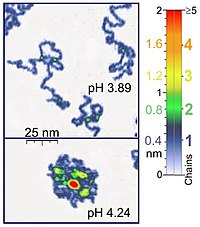
In tapping mode the cantilever is driven to oscillate up and down at near its resonance frequency by a small piezoelectric element mounted in the AFM tip holder. The amplitude of this oscillation is greater than 10 nm, typically 100 to 200 nm. Due to the interaction of forces acting on the cantilever when the tip comes close to the surface, Van der Waals force or dipole-dipole interaction, electrostatic forces, etc cause the amplitude of this oscillation to decrease as the tip gets closer to the sample. An electronic servo uses the piezoelectric actuator to control the height of the cantilever above the sample. The servo adjusts the height to maintain a set cantilever oscillation amplitude as the cantilever is scanned over the sample. A Tapping AFM image is therefore produced by imaging the force of the oscillating contacts of the tip with the sample surface. This is an improvement on conventional contact AFM, in which the cantilever just drags across the surface at constant force and can result in surface damage. Tapping mode is gentle enough even for the visualization of supported lipid bilayers or adsorbed single polymer molecules (for instance, 0.4 nm thick chains of synthetic polyelectrolytes) under liquid medium. At the application of proper scanning parameters, the conformation of single molecules remains unchanged for hours (Roiter and Minko, 2005).
[edit] Non-Contact Mode
Here the tip of the cantilever does not contact the sample surface. Instead, during scanning, it oscillates above the adsorbed fluid layer on the surface. The cantilever is oscillated at a frequency slightly above its resonance frequency. The amplitude is typically a few nanometers (<10nm). The van der Waals forces, which extend from 1nm to 10nm above the adsorbed fluid layer, or any other long range force which extends above the surface decreases the resonance frequency of the cantilever. The decrease in resonance frequency causes the amplitude of oscillation to decrease. The feedback loop maintains a constant oscillation amplitude or frequency by vertically moving the scanner at each (x,y) data point until a “setpoint” amplitude or frequency is reached. The distance the scanner moves vertically at each (x,y) data point is stored by the computer to form the topographic image of the sample surface.

[edit] AFM -Beam Deflection Detection
Laser light from a solid state diode is reflected off the back of the cantilever and collected by a position sensitive detector (PSD) consisting of two closely spaced photodiodes whose output signal is collected by a differential amplifier. Angular displacement of cantilever results in one photodiode collecting more light than the other photodiode, producing an output signal (the difference between the photodiode signals normalized by their sum) which is proportional to the deflection of the cantilever. It detects cantilever deflections <1Å (thermal noise limited). A long beam path (several cm) amplifies changes in beam angle.

[edit] Force spectroscopy
Another major application of AFM (besides imaging) is force spectroscopy, the measurement of force-distance curves. For this method, the AFM tip is extended towards and retracted from the surface as the static deflection of the cantilever is monitored as a function of piezoelectric displacement. These measurements have been used to measure nanoscale contacts, atomic bonding, Van der Waals forces, and Casimir forces, dissolution forces in liquids and single molecule stretching and rupture forces (Hinterdorfer & Dufrêne). Forces of the order of a few pico-Newton can now be routinely measured with a vertical distance resolution of better than 0.1 nanometer.
Problems with the technique include no direct measurement of the tip-sample separation and the common need for low stiffness cantilevers which tend to 'snap' to the surface. The snap-in can be reduced by measuring in liquids or by using stiffer cantilevers, but in the latter case a more sensitive deflection sensor is needed. By applying a small dither to the tip, the stiffness (force gradient) of the bond can be measured as well (Hoffmann et al.).
[edit] Identification of individual surface atoms

The AFM can be used to image and manipulate atoms and structures on a variety of surfaces. The atom at the apex of the tip "senses" individual atoms on the underlying surface when it forms incipient chemical bonds with each atom. Because these chemical interactions subtly alter the tip's vibration frequency, they can be detected and mapped.
Physicist Oscar Custance (Osaka University, Graduate School of Engineering, Osaka, Japan) and his team used this principle to distinguish between atoms of silicon, tin and lead on an alloy surface (Nature 2007, 446, 64).
The trick is to first measure these forces precisely for each type of atom expected in the sample. The team found that the tip interacted most strongly with silicon atoms, and interacted 23% and 41% less strongly with tin and lead atoms. Thus, each different type of atom can be identified in the matrix as the tip is moved across the surface.
Such a technique has been used now in biology and extended recently to cell biology. Forces corresponding to (i) the unbinding of receptor ligand couples (ii) unfolding of proteins (iii) cell adhesion at single cell scale have been gathered.
[edit] Advantages and disadvantages

The AFM has several advantages over the scanning electron microscope (SEM). Unlike the electron microscope which provides a two-dimensional projection or a two-dimensional image of a sample, the AFM provides a true three-dimensional surface profile. Additionally, samples viewed by AFM do not require any special treatments (such as metal/carbon coatings) that would irreversibly change or damage the sample. While an electron microscope needs an expensive vacuum environment for proper operation, most AFM modes can work perfectly well in ambient air or even a liquid environment. This makes it possible to study biological macromolecules and even living organisms. In principle, AFM can provide higher resolution than SEM. It has been shown to give true atomic resolution in ultra-high vacuum (UHV) and, more recently, in liquid environments. High resolution AFM is comparable in resolution to Scanning Tunneling Microscopy and Transmission Electron Microscopy.
A disadvantage of AFM compared with the scanning electron microscope (SEM) is the image size. The SEM can image an area on the order of millimetres by millimetres with a depth of field on the order of millimetres. The AFM can only image a maximum height on the order of micrometres and a maximum scanning area of around 150 by 150 micrometres.
Another inconvenience is that an incorrect choice of tip for the required resolution can lead to image artifacts. Traditionally the AFM could not scan images as fast as an SEM, requiring several minutes for a typical scan, while a SEM is capable of scanning at near real-time (although at relatively low quality) after the chamber is evacuated. The relatively slow rate of scanning during AFM imaging often leads to thermal drift in the image (Lapshin, 2004, 2007), making the AFM microscope less suited for measuring accurate distances between artifacts on the image. However, several fast-acting designs were suggested to increase microscope scanning productivity (Lapshin and Obyedkov, 1993) including what is being termed videoAFM (reasonable quality images are being obtained with videoAFM at video rate - faster than the average SEM). To eliminate image distortions induced by thermodrift, several methods were also proposed (Lapshin, 2004, 2007).
AFM images can also be affected by hysteresis of the piezoelectric material (Lapshin, 1995) and cross-talk between the (x,y,z) axes that may require software enhancement and filtering. Such filtering could "flatten" out real topographical features. However, newer AFM use real-time correction software (for example, feature-oriented scanning, Lapshin, 2004, 2007) or closed-loop scanners which practically eliminate these problems. Some AFM also use separated orthogonal scanners (as opposed to a single tube) which also serve to eliminate cross-talk problems.
Due to the nature of AFM probes, they cannot normally measure steep walls or overhangs. Specially made cantilevers can be modulated sideways as well as up and down (as with dynamic contact and non-contact modes) to measure sidewalls, at the cost of more expensive cantilevers and additional artifacts.
[edit] Piezoelectric Scanners
AFM scanners are made from piezoelectric material, which expands and contracts proportionally to an applied voltage. Whether they elongate or contract depends upon the polarity of the voltage applied. The scanner is constructed by combining independently operated piezo electrodes for X, Y, & Z into a single tube, forming a scanner which can manipulate samples and probes with extreme precision in 3 dimensions.

Scanners are characterized by their sensitivity which is the ratio of piezo movement to piezo voltage, i.e. by how much the piezo material extends or contracts per applied volt. Because of differences in material or size, the sensitivity varies from scanner to scanner.
Sensitivity varies non-linearly with respect to scan size. Piezo scanners exhibit more sensitivity at the end than at the beginning of a scan. This causes the forward and reverse scans to behave differently and display hysteresis between the two scan directions. This can be corrected by applying a non-linear voltage to the piezo electrodes to cause linear scanner movement and calibrating the scanner accordingly.
The sensitivity of piezoelectric materials decreases exponentially with time. This causes most of the change in sensitivity to occur in the initial stages of the scanner’s life. Piezoelectric scanners are run for approximately 48 hours before they are shipped from the factory so that they are past the point where we can expect large changes in sensitivity. As the scanner ages, the sensitivity will change less with time and the scanner would seldom require recalibration.
[edit] See also
| Wikibooks has a book on the topic of |
| Wikimedia Commons has media related to: Atomic force microscopy |
- Interfacial force microscope
- Friction force microscope
- Scanning tunneling microscope
- Scanning probe microscopy
- Scanning voltage microscopy
[edit] References
- A. D L. Humphris, M. J. Miles, J. K. Hobbs, A mechanical microscope: High-speed atomic force microscopy, Applied Physics Letters 86, 034106 (2005).
- D. Sarid, Scanning Force Microscopy, Oxford Series in Optical and Imaging Sciences, Oxford University Press, New York (1991)
- R. Dagani, Individual Surface Atoms Identified, Chemical & Engineering News, 5 March 2007, page 13. Published by American Chemical Society
- Q. Zhong, D. Inniss, K. Kjoller, V. B. Elings, Surf. Sci. Lett. 290, L688 (1993).
- V. J. Morris, A. R. Kirby, A. P. Gunning, Atomic Force Microscopy for Biologists. (Book) (December 1999) Imperial College Press.
- J. W. Cross SPM - Scanning Probe Microscopy Website
- P. Hinterdorfer, Y. F. Dufrêne, Nature Methods, 3, 5 (2006)
- F. Giessibl, Advances in Atomic Force Microscopy, Reviews of Modern Physics 75 (3), 949-983 (2003).
- R. H. Eibl, V.T. Moy, Atomic force microscopy measurements of protein-ligand interactions on living cells. Methods Mol Biol. 305:439-50 (2005)
- P. M. Hoffmann, A. Oral, R. A. Grimble, H. Ö. Özer, S. Jeffery, J. B. Pethica, Proc. Royal Soc. A 457, 1161 (2001).
- R. V. Lapshin, O. V. Obyedkov, Fast-acting piezoactuator and digital feedback loop for scanning tunneling microscopes, Review of Scientific Instruments, vol. 64, no. 10, pp. 2883-2887, 1993.
- R. V. Lapshin, Analytical model for the approximation of hysteresis loop and its application to the scanning tunneling microscope, Review of Scientific Instruments, vol. 66, no. 9, pp. 4718-4730, 1995.
- R. V. Lapshin, Feature-oriented scanning methodology for probe microscopy and nanotechnology, Nanotechnology, vol. 15, iss. 9, pp. 1135-1151, 2004.
- R. V. Lapshin, Automatic drift elimination in probe microscope images based on techniques of counter-scanning and topography feature recognition, Measurement Science and Technology, vol. 18, iss. 3, pp. 907-927, 2007.
- P. West, Introduction to Atomic Force Microscopy: Theory, Practice and Applications --- www.AFMUniversity.org
- R. W. Carpick and M. Salmeron, Scratching the surface: Fundamental investigations of tribology with atomic force microscopy, Chemical Reviews, vol. 97, iss. 4, pp. 1163-1194 (2007).
- Y. Roiter and S. Minko, AFM Single Molecule Experiments at the Solid-Liquid Interface: In Situ Conformation of Adsorbed Flexible Polyelectrolyte Chains, Journal of the American Chemical Society, vol. 127, iss. 45, pp. 15688-15689 (2005).
|
||||||||||||||||


